...
| Page properties |
|---|
|
Note for Download Link of the Scroll ignore macro: |
| Scroll pdf ignore |
|---|
Table of Contents |
...
- 3 x Samtec ASP-122953-01 160-pin stackable, compatible with TE0782TE078x
- 2 mm MC LB2-A soldered Soldered Connector for power supply (12V input)
- 4 SMA connectors for MGT (1xTX 1xRX)
- 2 x 12 pin headers for XMOD
- 1 x DIP switch for modules CPLD Access
- 2 x RJ45 Connector
- USB A Stacked Connector
- Equipped with two TE0790 XMOD FTDI JTAG adapters, TE0790 and TE0790-xxL
- Voltage regulator for 5V and 3.3Vregulators
- Dimension: 115 x 115 mm
- Two preassembled TE0790 XMOD FTDI JTAG adapters
Block Diagram
| Page properties |
|---|
|
add drawIO object here.
|
...
| Scroll Title |
|---|
| anchor | Figure_OV_BD |
|---|
| title | TEBT0782 block diagram |
|---|
|
| Scroll Ignore |
|---|
| draw.io Diagram |
|---|
| border | false |
|---|
| viewerToolbar | true |
|---|
| |
|---|
| fitWindow | false |
|---|
| diagramDisplayName | |
|---|
| lbox | true |
|---|
| revision | 712 |
|---|
| diagramName | TEBT0782_OV_BD |
|---|
| simpleViewer | false |
|---|
| width | |
|---|
| links | auto |
|---|
| tbstyle | hidden |
|---|
| diagramWidth | 641 |
|---|
|
|
| Scroll Only |
|---|
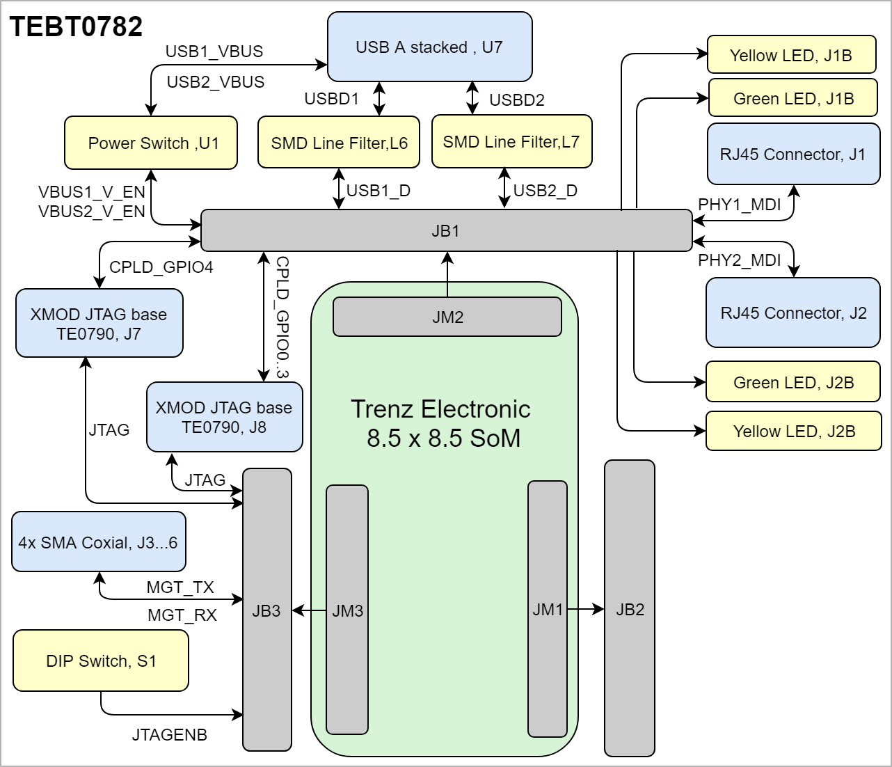 Image Modified Image Modified
|
|
Main Components
...
| Scroll Title |
|---|
| anchor | Figure_OV_MC |
|---|
| title | TEBT0782 main components |
|---|
|
| Scroll Ignore |
|---|
| draw.io Diagram |
|---|
| border | false |
|---|
| viewerToolbar | true |
|---|
| |
|---|
| fitWindow | false |
|---|
| diagramDisplayName | |
|---|
| lbox | true |
|---|
| revision | 58 |
|---|
| diagramName | TEBT0782_OV_MC |
|---|
| simpleViewer | false |
|---|
| width | |
|---|
| links | auto |
|---|
| tbstyle | hidden |
|---|
| diagramWidth | 440 |
|---|
|
|
| Scroll Only |
|---|
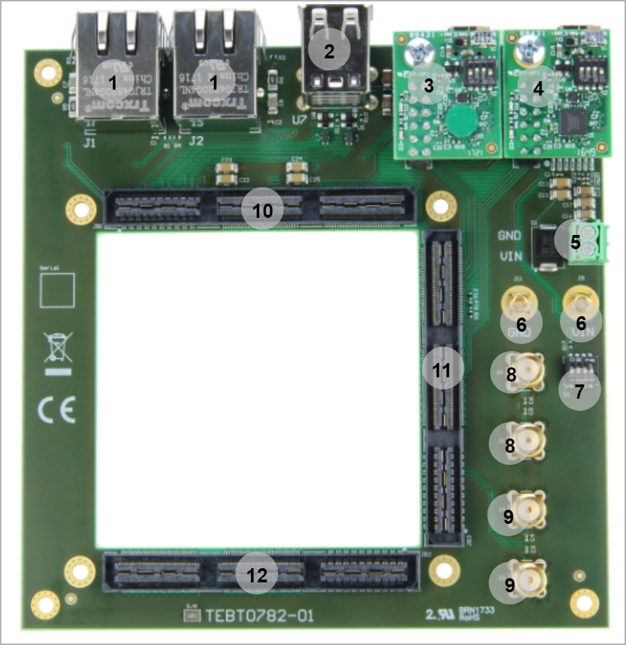 Image Modified Image Modified
|
|
- RJ45 Transceivers, J1-J2
- USB A Stacked, U7
- XMOD JTAG/UART BaseAdapter, J7
- JTAG CPLD Adapter -J8
- 2 Line Common Mode Choke, J10
- Non-isolated power jack (VIN), J9-J11
- DIP Switch, S1
- SMA Coxial Connectors (MGT_TX), J3-J4
- SMA Coxial Connectors (MGT_RX), J5-, J3...J6
- Board to Board ConnectorsConnector, JB1...JB3
- Board to Board Connector, JB3
- Board to Board Connector, JB2
Initial Initial Delivery State
| Page properties |
|---|
|
Notes : Only components like EEPROM, QSPI flash and DDR3 can be initialized by default at manufacture. If there is no components which might have initial data ( possible on carrier) you must keep the table empty |
...
| Page properties |
|---|
|
- Overview of Boot Mode, Reset, Enables.
|
The general Reset is provided through button S1 on TE0790 XMOD J7.
| Scroll Title |
|---|
| anchor | Table_OV_RST |
|---|
| title | Reset process. |
|---|
|
| Scroll Table Layout |
|---|
| orientation | portrait |
|---|
| sortDirection | ASC |
|---|
| repeatTableHeaders | default |
|---|
| style | |
|---|
| widths | |
|---|
| sortByColumn | 1 |
|---|
| sortEnabled | false |
|---|
| cellHighlighting | true |
|---|
|
Signal | B2B | Note |
|---|
RESIN | JBC3-130 | Board Reset |
|
...
| Page properties |
|---|
|
Notes : - For carrier or stand-alone boards use subsection for every connector type (add designator Designator on description, not on the subsection title), for example:
- For modules which needs carrier use only classes and refer to B2B connector if more than one is used, for example
|
...
| Scroll Title |
|---|
| anchor | Table_SIP_B2B |
|---|
| title | General PL I/O to B2B connectors information |
|---|
|
| Scroll Table Layout |
|---|
| orientation | portrait |
|---|
| sortDirection | ASC |
|---|
| repeatTableHeaders | default |
|---|
| style | |
|---|
| widths | |
|---|
| sortByColumn | 1 |
|---|
| sortEnabled | false |
|---|
| cellHighlighting | true |
|---|
|
| B2B Connector | Interface | Number of I/O | Notes | JBC1
|---|
JB1
| RJ45, J1B-J1C | 1 Differential pair, 2 Single Ended | Yellow, Green LEDs | | RJ45, J1A | 4 Differential pair, 8 Single Ended | PHY1 MDIO | | RJ45, J2B-J2C | 1 Differential pair, 2 Single Ended | Yellow, Green LEDs | | RJ45, J2A | 4 Differential pair, 8 Single Ended | PHY2 MDIO | | TE0790 Base, J8 | 4 Single Ended |
| | TE0790 Base, J7 | 1 Single Ended |
| | USB A Stacked, U7 | 2 Single Ended | USB | | Power Switch, U1 | 2 Single Ended |
| | SMD Line Filter, L6 | 1 Differential pair, 2 Single Ended | USB1_D | | SMD Line Filter, L7 | 1 Differential pair, 2 Single Ended | JBC2
USB2_D | | ESD protection diode, U5 | 1 | Module TE0782...4 FPGA, Bank 111-112 | 16 Differential pair, 32 Single Ended | USB1_VBUS | | ESD protection diode, U8 | 1 Single Ended | USB2_VBUS | JB2
| Module TE078x FPGA, Bank 111-112 | 16 Differential pair, 32 Single Ended | MGT_RX8MGT_RX8...15, MGT_TX8...15 | | Module TE0782...4 TE078x FPGA, Bank 34 | 1 Differential pair, 2 Single Ended | J1_B34_VRP, J1_B34_VRN | | Module TE0782...4 TE078x FPGA, Bank 34 | 1 Differential pair, 2 Single Ended | J1_B33_VRP, J1_B33_VRNJBC3 | JB3
| TE0790 Base, J8 | 4 Single Ended | M_TCK, M_TMS, M_TDO, M_TDI | | TE0790 Base, J7 | 4 Single Ended 2 Single Ended 1 Single Ended | TCK, TMS, TDO, TDI UART RX/TX RESIN | | DIP Switch, S1-A | 1 Single Ended | JTAGENB | | SMA Coaxial, J3...6 | 2 Differential pair, 4 Single Ended | MGT_RX0, MGT_TX0 | | Module TE0782...4 FPGA, Bank 109-110 | 16 Differential pair, 32 Single Ended | MGT_RX1...7, MGT_TX0...7 |
|
JTAG Interface
JTAG/UART to Module SoC/FPGA
JTAG access to the TE078x SoM is Two JTAG accesses to the TEBT0782 SoMs are available through B2B connector JB3. JTAGENB is connected to DIP Switch S1-A JTAG access is provided by TE0790 XMOD Adapter on Pin Header J7.
| Scroll Title |
|---|
| anchor | Table_SIP_JTG |
|---|
| title | JTAG pins connection |
|---|
|
| Scroll Table Layout |
|---|
| orientation | portrait |
|---|
| sortDirection | ASC |
|---|
| repeatTableHeaders | default |
|---|
| style | |
|---|
| widths | |
|---|
| sortByColumn | 1 |
|---|
| sortEnabled | false |
|---|
| cellHighlighting | true |
|---|
|
TE0790 BaseJTAG | Signal Name | B2B Connector | Notes |
|---|
J8TMS142TDI147TDOJB3C-148J8 | M_TMS | JB3B-182 | M_TDI | JB3B-187 | M_TDO | JB3B-188 | M_TCK | JB3B-181 | |
UART
...
| anchor | Table_SIP_UART |
|---|
| title | UART Pins |
|---|
...
Signal State
...
XMOD_B
...
| JTAG | | D | TDO | JB3C-148 | JTAG | | E | CPLD_GPIO4 | JB1A-18 |
| | F | TDI | JB3C-147 | JTAG | | G | RESIN | JB3C-130 | General Reset | | H | TMS | JB3C-142 | JTAG | | 3.3V | 3.3V_M | JB1- JB3 |
| | VIO | 3.3V_M | JB1- JB3 | 3.3V |
|
JTAG/ GPIO to Module CPLD
JTAG access to the System Controller CPLD is provided through B2B connector J3. JTAG access to CPLD is provided by TE0790 XMOD Adapter on Pin Header J8.
Pin 'JTAGENB' must be set high, using DIP Switch S1-A in order to program the System Controller CPLD via JTAG interaface.
| Scroll Title |
|---|
| anchor | Table_SIP_CPLDJTG |
|---|
| title | CPLD JTAG pins connection |
|---|
|
RJ45 Connectors
| Scroll Title |
|---|
| anchor | Table_SIP_RJ45 |
|---|
| title | RJ45s Connections to B2B Connectors |
|---|
|
| Scroll Table Layout |
|---|
| orientation | portrait |
|---|
| sortDirection | ASC |
|---|
| repeatTableHeaders | default |
|---|
| style | |
|---|
| widths | |
|---|
| sortByColumn | 1 |
|---|
| sortEnabled | false |
|---|
| cellHighlighting | true |
|---|
|
JTAG Interface Pins | Signal Name |
|---|
RJ45-J1 | RJ45-J2 Pin | B2BPHYMDI0_P23JB1A-39PHYMDI0_N21JB1A-37PHYMDI1_PJB1A19JB1A-35PHYMDI1_NJB1A17JB1A-33PHYMDI2_P15JB1A-31PHYMDI2_NJB1A13JB1A-29PHYMDI3_P11JB1A-27PHYMDI3_NJB1A9JB1A-25 | | J2_TX9_P | JB1A-95 | - | LED Green/Yellow | | J2_TX9_N | JB1A-97 | - | LED Green/Yellow | | J2_RX9_N | - | JB1A-96 | LED Green/Yellow | | J2_RX9_P | - | JB1A-98 | LED Green/Yellow | |
USB A Stacked
The USB A Stacked, U7 is a dual port USB Socket which provides two USB connectors.
| 82 |
| | 3.3V | 3.3V_CPLD | JB1- JB3 |
| | VIO | 3.3V_CPLD | JB1- JB3 | 3.3V |
|
DIP Switch S2 on TE0790 must be set and fixed like the following table.
| Scroll Title |
|---|
| anchor | Table_SIP_JTG_DIP |
|---|
| title | XMOD DIP Switch Setting |
|---|
|
| Scroll Title |
|---|
| anchor | Table_SIP_USB |
|---|
| title | Dual Port USB Connections |
|---|
|
| Scroll Table Layout |
|---|
| orientation | portrait |
|---|
| sortDirection | ASC |
|---|
| repeatTableHeaders | default |
|---|
| style | |
|---|
| widths | |
|---|
| sortByColumn | 1 |
|---|
| sortEnabled | false |
|---|
| cellHighlighting | true |
|---|
|
|
| Signal Name | Port A | Port B | Notes |
|---|
| B2B | Connected to | B2B | Connected to |
|---|
USB_D_P | JB1A-28 | SMD Line Filter, L7 | JB1A-40 | SMD Line Filter, L6 | USB_D_N | JB1A-26 | SMD Line Filter, L7 | JB1A-38 | SMD Line Filter, L6 | USB_VBUS | JB1A-24 | SMD Line Filter, L7 | JB1A-36 | SMD Line Filter, L6 | VBUS_V_EN | JB1A-30 | Power Switch, U1 | JB1A-32 | Power Switch, U1 |
SMA Coaxial
The TEBT0782 carrier is equipped with 4 SMA Coaxial connectors.
DIP Switch | Setting | Notes |
|---|
| S2-1 | ON | JTAGENB (Enable/Disable module JTAG CPLD IOs) | | S2-2 | OFF | NC | | S2-3 | OFF | NC | | S2-4 | OFF | NC |
|
RJ45 Connectors
| Scroll Title |
|---|
| anchor | Table_SIP_RJ45 |
|---|
| title | RJ45s Connections to B2B Connectors |
|---|
|
| Scroll Table Layout |
|---|
| orientation | portrait |
|---|
| sortDirection | ASC |
|---|
| repeatTableHeaders | default |
|---|
| style | |
|---|
| widths | |
|---|
| sortByColumn | 1 |
|---|
|
|
| Scroll Title |
|---|
| anchor | Table_SIP_SMA |
|---|
| title | SMAs Connections |
|---|
|
| Scroll Table Layout |
|---|
| orientation | portrait |
|---|
| sortDirection | ASC |
|---|
| repeatTableHeaders | default |
|---|
style | widths | | sortByColumn | 1 |
|---|
| sortEnabled | false |
|---|
| cellHighlighting | true |
|---|
|
| Signal Name | RJ45-J1 Pin | RJ45-J2 Pin |
|---|
Designator | Schematic | B2BJ3MGTTX0NJB3A-29 | J4 | | JB1A-23 | JB1A-39 |
| | PHY_MDI0_N | JB1A-21 | JB1A-37 |
| | PHY_MDI1 |
MGT_TX0JB3A31J5MGTRX0JB3A30J6MGTRX0JB3A32 |
...
...
| 31 |
| | PHY_MDI2_N | JB1A-13 | JB1A-29 |
| | PHY_MDI3_P | JB1A-11 | JB1A-27 |
| | PHY_MDI3_N | JB1A-9 | JB1A-25 |
| | J2_TX9_P | JB1A-95 | - | LED Green/Yellow | | J2_TX9_N | JB1A-97 | - | LED Green/Yellow | | J2_RX9_N | - | JB1A-96 | LED Green/Yellow | | J2_RX9_P | - | JB1A-98 | LED Green/Yellow |
|
USB A Stacked Socket
The USB A Stacked (U7) is a dual port USB Socket which provides two USB ports.
| Page properties |
|---|
|
Notes : - add subsection for every component which is important for design, for example:
- Two 100 Mbit Ethernet Transciever PHY
- USB PHY
- Programmable Clock Generator
- Oscillators
- eMMCs
- RTC
- FTDI
- ...
- DIP-Switches
- Buttons
- LEDs
|
| Page properties |
|---|
|
Notes : In the on-board peripheral table "chip/Interface" must be linked to the corresponding chapter or subsection |
...
| anchor | Table_OBP |
|---|
| title | On board peripherals |
|---|
...
DIP Switch
| Scroll Title |
|---|
| anchor | Table_OBPSIP_DIPUSB |
|---|
| title | DIP Switch Dual Port USB Connections |
|---|
|
| Scroll Table Layout |
|---|
| orientation | portrait |
|---|
| sortDirection | ASC |
|---|
| repeatTableHeaders | default |
|---|
| style | |
|---|
| widths | |
|---|
| sortByColumn | 1 |
|---|
| sortEnabled | false |
|---|
| cellHighlighting | true |
|---|
|
| Signal Name | Port A | Port B | Notes |
|---|
| B2B | Connected |
|---|
Switch | Connected Notes | S1A | JTABENB | JB3C-36 | |
Power and Power-On Sequence
...
In 'Power and Power-on Sequence' section there are three important digrams which must be drawn:
- Power on-sequence
- Power distribution
- Voltage monitoring circuit
| Note |
|---|
For more information regarding how to draw diagram, Please refer to "Diagram Drawing Guidline" . |
| Connected to |
|---|
| USB_D_P | JB1A-28 | SMD Line Filter, L7 | JB1A-40 | SMD Line Filter, L6 |
| | USB_D_N | JB1A-26 | SMD Line Filter, L7 | JB1A-38 | SMD Line Filter, L6 |
| | USB_VBUS | JB1A-24 | SMD Line Filter, L7 | JB1A-36 | SMD Line Filter, L6 |
| | VBUS_V_EN | JB1A-30 | Power Switch, U1 | JB1A-32 | Power Switch, U1 |
|
|
SMA Coaxial
The TEBT0782 carrier is equipped with 4x SMA Coaxial straight connectors.
Power Supply
Power supply with minimum current capability of 2.5 A for system startup is recommended.
...
| Scroll Title |
|---|
| anchor | Table_PWRSIP_PCSMA |
|---|
| title | Power ConsumptionSMAs Connections |
|---|
|
| Scroll Table Layout |
|---|
| orientation | portrait |
|---|
| sortDirection | ASC |
|---|
| repeatTableHeaders | default |
|---|
| style | |
|---|
| widths | |
|---|
| sortByColumn | 1 |
|---|
| sortEnabled | false |
|---|
| cellHighlighting | true |
|---|
|
|
| Power Input Pin | Typical Current |
|---|
| VIN | TBD* |
* TBD - To Be Determined
Power Distribution Dependencies
...
| anchor | Figure_PWR_PD |
|---|
| title | Power Distribution |
|---|
...
| scroll-pdf | false |
|---|
| scroll-office | true |
|---|
| scroll-chm | true |
|---|
| scroll-docbook | true |
|---|
| scroll-eclipsehelp | true |
|---|
| scroll-epub | true |
|---|
| scroll-html | true |
|---|
...
| Scroll Only |
|---|
 Image Removed Image Removed
|
Power-On Sequence
...
| anchor | Figure_PWR_PS |
|---|
| title | Power Sequency |
|---|
...
| Scroll Only |
|---|
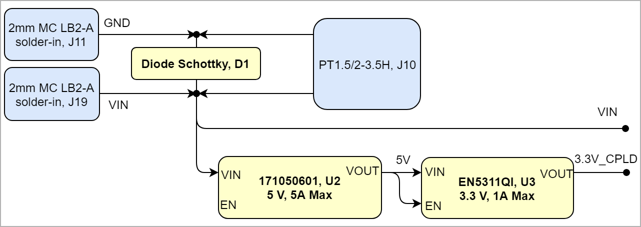 Image Removed Image Removed
|
Voltage Monitor Circuit
...
| anchor | Figure_PWR_VMC |
|---|
| title | Voltage Monitor Circuit |
|---|
| Scroll Ignore |
|---|
Create DrawIO object here: Attention if you copy from other page, objects are only linked. |
| Scroll Only |
|---|
image link to the generate DrawIO PNG file of this page. This is a workaround until scroll pdf export bug is fixed |
Power Rails
...
| anchor | Table_PWR_PR |
|---|
| title | Module power rails. |
|---|
...
B2B JM1 Pin
...
B2B JM2 Pin
...
B2B JM3 Pin
...
VCCIO33
...
...
use "include page" macro and link to the general B2B connector page of the module series,
...
? x ? modules use two or three Samtec Micro Tiger Eye Connector on the bottom side.
3 x REF-??????? (compatible to ????????), (?? pins, ?? per row)
| Designator | Schematic | B2B | Notes |
|---|
| J3 | MGT_TX0_N | JB3A-29 | Transfer | | J4 | MGT_TX0_P | JB3A-31 | Transfer | | J5 | MGT_RX0_N | JB3A-30 | Receive | | J6 | MGT_RX0_P | JB3A-32 | Receive |
|
Test Points
| Scroll Title |
|---|
| anchor | Table_SIP_TestPoint |
|---|
| title | Test Points Information |
|---|
|
| Scroll Table Layout |
|---|
| orientation | portrait |
|---|
| sortDirection | ASC |
|---|
| repeatTableHeaders | default |
|---|
| style | |
|---|
| widths | |
|---|
| sortByColumn | 1 |
|---|
| sortEnabled | false |
|---|
| cellHighlighting | true |
|---|
|
Test Point | Signals | B2B Connector | Notes |
|---|
| TP 1 | VBAT_I | JB3-124 |
| | TP 2 | OTG2_ID | JB1-22 |
| | TP 3 | OTG1_ID | JB1-34 |
| | TP 4 | USB1_VBUS | JB1-36 |
| | TP 5 | USB2_VBUS | JB1-24 |
| | TP 6 | M_TCK | JB3-81 |
| | TP 7 | M_TDO | JB3-88 |
| | TP 8 | M_TDI | JB3-87 |
| | TP 9 | M_TMS | JB3-82 |
| | TP 10 | TCK | JB3-141 |
| | TP 11 | TDO | JB3-148 |
| | TP 12 | TDI | JB3-147 |
| | TP 13 | TMS | JB3-142 |
| | TP 14 | VIN | JB1-165...168 |
| | TP 15 | 5V | - |
| | TP 16 | 3.3V_CPLD | JB1-147...148 |
| | TP 17-18 | GND | - |
|
|
On-board Peripherals
| Page properties |
|---|
|
Notes : - add subsection for every component which is important for design, for example:
- Two 100 Mbit Ethernet Transciever PHY
- USB PHY
- Programmable Clock Generator
- Oscillators
- eMMCs
- RTC
- FTDI
- ...
- DIP-Switches
- Buttons
- LEDs
|
| Page properties |
|---|
|
Notes : In the on-board peripheral table "chip/Interface" must be linked to the corresponding chapter or subsection |
| Scroll Title |
|---|
| anchor | Table_OBP |
|---|
| title | On board peripherals |
|---|
|
| Scroll Table Layout |
|---|
| orientation | portrait |
|---|
| sortDirection | ASC |
|---|
| repeatTableHeaders | default |
|---|
| style | |
|---|
| widths | |
|---|
| sortByColumn | 1 |
|---|
| sortEnabled | false |
|---|
| cellHighlighting | true |
|---|
|
|
DIP Switch
| Scroll Title |
|---|
| anchor | Table_OBP_DIP |
|---|
| title | DIP Switch Connections |
|---|
|
| Scroll Table Layout |
|---|
| orientation | portrait |
|---|
| sortDirection | ASC |
|---|
| repeatTableHeaders | default |
|---|
| style | |
|---|
| widths | |
|---|
| sortByColumn | 1 |
|---|
| sortEnabled | false |
|---|
| cellHighlighting | true |
|---|
|
| Switch | Connected to | B2B | Notes |
|---|
| S1-A | JTABENB | JB3C-136 |
| | S1-B...D | - | - | Not connected |
|
Power and Power-On Sequence
| Page properties |
|---|
|
In 'Power and Power-on Sequence' section there are three important digrams which must be drawn: - Power on-sequence
- Power distribution
- Voltage monitoring circuit
|
Power Supply
Power supply with minimum current capability of 3A for system startup is recommended.
Power Consumption
| Scroll Title |
|---|
| anchor | Table_PWR_PC |
|---|
| title | Power Consumption |
|---|
|
| Scroll Table Layout |
|---|
| orientation | portrait |
|---|
| sortDirection | ASC |
|---|
| repeatTableHeaders | default |
|---|
| style | |
|---|
| widths | |
|---|
| sortByColumn | 1 |
|---|
| sortEnabled | false |
|---|
| cellHighlighting | true |
|---|
|
| Power Input Pin | Typical Current |
|---|
| VIN | TBD* |
|
* TBD - To Be Determined
Power Distribution Dependencies
12V power supply (VIN) on J9/J11 (2 mm MC LB2-A solder-in) or on J10 (TE1.5/2-3.5H).
| Scroll Title |
|---|
| anchor | Figure_PWR_PD |
|---|
| title | Power Distribution |
|---|
|
| Scroll Ignore |
|---|
| scroll-pdf | false |
|---|
| scroll-office | true |
|---|
| scroll-chm | true |
|---|
| scroll-docbook | true |
|---|
| scroll-eclipsehelp | true |
|---|
| scroll-epub | true |
|---|
| scroll-html | true |
|---|
| | draw.io Diagram |
|---|
| border | false |
|---|
| viewerToolbar | true |
|---|
| |
|---|
| fitWindow | false |
|---|
| diagramDisplayName | |
|---|
| lbox | true |
|---|
| revision | 7 |
|---|
| diagramName | TEBT0784_PWR_PD |
|---|
| simpleViewer | false |
|---|
| width | |
|---|
| links | auto |
|---|
| tbstyle | hidden |
|---|
| diagramWidth | 641 |
|---|
|
|
| Scroll Only |
|---|
 Image Added Image Added
|
|
Power-On Sequence
| Scroll Title |
|---|
| anchor | Figure_PWR_PS |
|---|
| title | Power Sequency |
|---|
|
| Scroll Ignore |
|---|
| draw.io Diagram |
|---|
| border | false |
|---|
| viewerToolbar | true |
|---|
| |
|---|
| fitWindow | false |
|---|
| diagramDisplayName | |
|---|
| lbox | true |
|---|
| revision | 9 |
|---|
| diagramName | TEBT0782_PWR_PS |
|---|
| simpleViewer | false |
|---|
| width | |
|---|
| links | auto |
|---|
| tbstyle | hidden |
|---|
| diagramWidth | 641 |
|---|
|
|
| Scroll Only |
|---|
Image Added |
|
Power Rails
| Scroll Title |
|---|
| anchor | Table_PWR_PR |
|---|
| title | Module power rails. |
|---|
|
| Scroll Table Layout |
|---|
| orientation | portrait |
|---|
| sortDirection | ASC |
|---|
| repeatTableHeaders | default |
|---|
| style | |
|---|
| widths | |
|---|
| sortByColumn | 1 |
|---|
| sortEnabled | false |
|---|
| cellHighlighting | true |
|---|
|
| Power Rail Name | B2B JB1 Pin | B2B JB2 Pin | B2B JB3 Pin | Direction | Notes |
|---|
| VIN | 165, 166, 167, 168 | - | - | Input/Output | Directly to module | | 3.3V_M | 99, 100, 111,112, 123, 124, 135, 136, 159, 160, 169, 170, 171, 172 | - | 99, 100, 159, 160 | Input/Output | 160, 169, 170, 171, 172 are output other ones input for IO Banks | | 3.3V_CPLD | 147,148 | - | - | Output | Directly to module | | 1.8V_M | - | 99,100, 159, 160, 169, 170, 171, 172 | 124 | Input/Output | 169, 170, 171, 172 are output other ones input for IO Banks | | VBAT_IN |
|
|
|
|
|
|
Board to Board Connectors
| Page properties |
|---|
|
- This section is optional and only for modules.
use "include page" macro and link to the general B2B connector page of the module series, For example: 6 x 6 SoM LSHM B2B Connectors
| Include Page |
|---|
| 6 x 6 SoM LSHM B2B Connectors |
|---|
| 6 x 6 SoM LSHM B2B Connectors |
|---|
|
|
| Include Page |
|---|
| 8.5 x 8.5 SoM QSH and QTH B2B Connectors |
|---|
| 8.5 x 8.5 SoM QSH and QTH B2B Connectors |
|---|
|
...
Technical Specifications
Absolute Maximum Ratings
| Scroll Title |
|---|
| anchor | Table_TS_AMR |
|---|
| title | PS absolute maximum ratings |
|---|
|
| Scroll Table Layout |
|---|
| orientation | portrait |
|---|
| sortDirection | ASC |
|---|
| repeatTableHeaders | default |
|---|
| style | |
|---|
| widths | |
|---|
| sortByColumn | 1 |
|---|
| sortEnabled | false |
|---|
| cellHighlighting | true |
|---|
|
|
| Symbols | Description | Min | Max | Unit |
|---|
V | | false |
|---|
| cellHighlighting | true |
|---|
|
| Symbols | Description | Min | Max | Unit | Note |
|---|
| VIN | Input supply voltage | -- | -- | V | Attention: Depends on connected module! 171050601 of the TEBT0782 (-0,3V - 40V) |
| T_STG | Storage Temperature | -40 | +85 | °C | DIP Switch S1 |
Recommended Operating Conditions
...
| Scroll Title |
|---|
| anchor | Table_TS_ROC |
|---|
| title | Recommended operating conditions. |
|---|
|
| Scroll Table Layout |
|---|
| orientation | portrait |
|---|
| sortDirection | ASC |
|---|
| repeatTableHeaders | default |
|---|
| style | |
|---|
| widths | |
|---|
| sortByColumn | 1 |
|---|
| sortEnabled | false |
|---|
| cellHighlighting | true |
|---|
|
| Parameter | Min | Max | Units | Reference Document |
|---|
| VIN | 11.4 | 12.6 | V |
See Xilinx ???? datasheet. | °C | | Attention: Depends on connected module! See TE078x TRMs, recommended normally 12V Without module: 171050601 of the TEBT0782 (6V - 36V) | | T_OPT | -40 | +85 | °C |
See Xilinx ???? datasheet.
|
Physical Dimensions
Module size: 116 mm × 116 mm. Please download the assembly diagram for exact numbers.
Mating height with standard connectors: ? 5 mm.
PCB thickness: 1.6 mm.
...
| Scroll Title |
|---|
| anchor | Figure_TS_PD |
|---|
| title | Physical Dimension |
|---|
|
| Scroll Ignore |
|---|
| draw.io Diagram |
|---|
| border | false |
|---|
| viewerToolbar | true |
|---|
| |
|---|
| fitWindow | false |
|---|
| diagramDisplayName | |
|---|
| lbox | true |
|---|
| revision | 1 |
|---|
| diagramName | TEBT0782_TS_PD |
|---|
| simpleViewer | false |
|---|
| width | |
|---|
| links | auto |
|---|
| tbstyle | hidden |
|---|
| diagramWidth | 641 |
|---|
|
|
| Scroll Only |
|---|
| scroll-pdf | true |
|---|
| scroll-office | true |
|---|
| scroll-chm | true |
|---|
| scroll-docbook | true |
|---|
| scroll-eclipsehelp | true |
|---|
| scroll-epub | true |
|---|
| scroll-html | true |
|---|
| 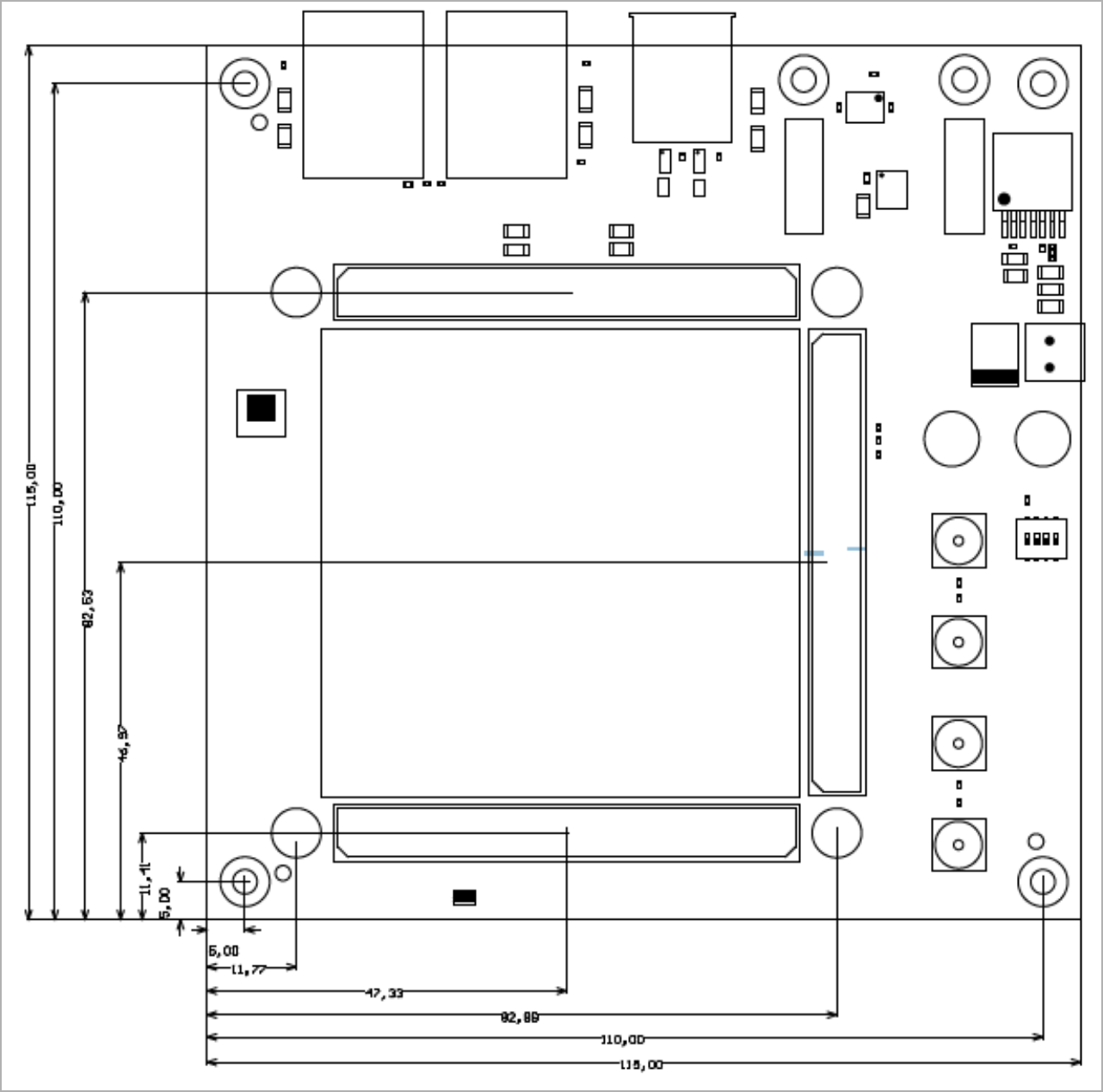 Image Modified Image Modified
|
|
Currently Offered Variants
...
| Scroll Title |
|---|
| anchor | Table_RH_HRH |
|---|
| title | Hardware Revision History |
|---|
|
| Scroll Table Layout |
|---|
| orientation | portrait |
|---|
| sortDirection | ASC |
|---|
| repeatTableHeaders | default |
|---|
| style | |
|---|
| widths | |
|---|
| sortByColumn | 1 |
|---|
| sortEnabled | false |
|---|
| cellHighlighting | true |
|---|
|
| Date | Revision | Changes | Documentation Link |
|---|
| 302016-1011-201605 | 01- | Initial Release | REV01 |
|
Hardware revision number can be found on the PCB board together with the module model number separated by the dash.
| Scroll Title |
|---|
| anchor | Figure_RV_HRN |
|---|
| title | Board hardware revision number. |
|---|
|
| Scroll Ignore |
|---|
| draw.io Diagram |
|---|
| border | false |
|---|
| viewerToolbar | true |
|---|
| |
|---|
| fitWindow | false |
|---|
| diagramDisplayName | |
|---|
| lbox | true |
|---|
| revision | 24 |
|---|
| diagramName | TEBT0782_RH_HRN |
|---|
| simpleViewer | false |
|---|
| width | |
|---|
| links | auto |
|---|
| tbstyle | hidden |
|---|
| diagramWidth | 143203 |
|---|
|
|
| Scroll Only |
|---|

|
|
Document Change History
...
| Scroll Title |
|---|
| anchor | Table_RH_DCH |
|---|
| title | Document change history. |
|---|
|
| Scroll Table Layout |
|---|
| orientation | portrait |
|---|
| sortDirection | ASC |
|---|
| repeatTableHeaders | default |
|---|
| style | |
|---|
| widths | |
|---|
| sortByColumn | 1 |
|---|
| sortEnabled | false |
|---|
| cellHighlighting | true |
|---|
|
| Date | Revision | Contributor | Description |
|---|
| Page info |
|---|
| infoType | Modified date |
|---|
| dateFormat | yyyy-MM-dd |
|---|
| type | Flat |
|---|
|
| | Page info |
|---|
| infoType | Current version |
|---|
| prefix | v. |
|---|
| type | Flat |
|---|
| showVersions | false |
|---|
|
| | Page info |
|---|
| infoType | Modified by |
|---|
| type | Flat |
|---|
| showVersions | false |
|---|
|
| | | 2019-10-8 | v.45 | John Hartfiel | update power section - XMOD section
| | 2019-10-16 | v.44 | Pedram Babakhani | | -- | all | | Page info |
|---|
| infoType | Modified users |
|---|
| type | Flat |
|---|
| showVersions | false |
|---|
|
| |
|
...