...
- Xilinx Kintex-7 XC7K160T, XC7K325T or XC7K410T FPGA SoC
- Large number of configurable I/Os are provided via HPC FMC connector
- 4 GTX high-performance transceiver
- 2x MGT transceiver clock inputs
- 160 FPGA I/O's (80 LVDS pairs)
- On-board high-efficiency switch-mode DC-DC converters
- Lattice MachXO2 LCMXO2-1200HC System Controller CPLD
- 10x User LEDs
- PCI Express x8 connector with 4 lane PCIe Gen 2 interface
- ANSI Vita 57.1 FMC High Pin Count (HPC) connector
- DDR3 SODIMM SDRAM with ECC socket with 64bit databus width
- 256Mbit (32MByte) Quad SPI Flash memory (for configuration and operation) accessible through:
- FPGA
- JTAG port (SPI indirect, bus width x4)
- FPGA configuration through:
- JTAG connector
- Quad SPI Flash memory
Clocking
- System management and power sequencing
...
| Scroll Title |
|---|
| anchor | Figure_OV_MC |
|---|
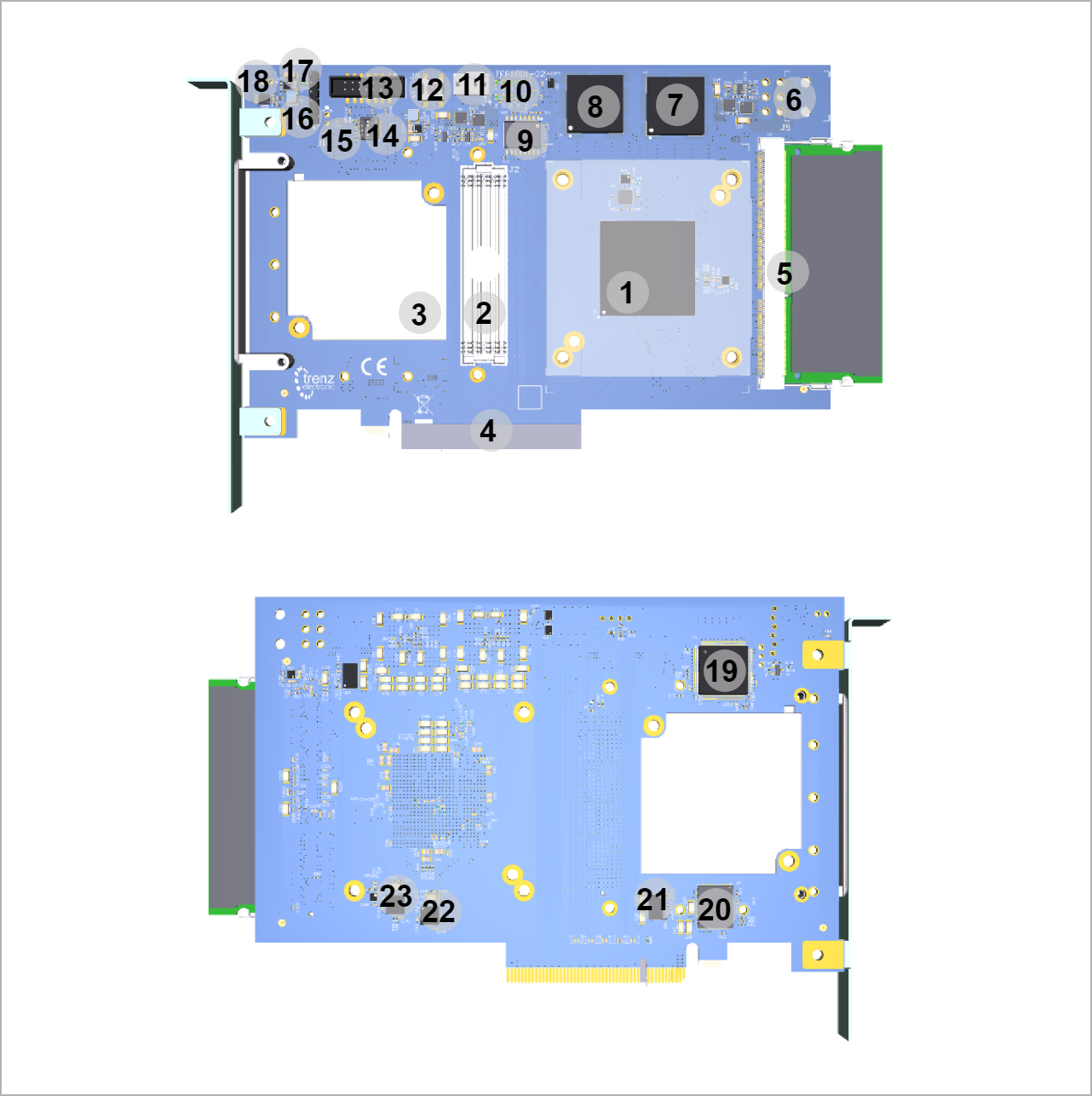
| title | TEF1001-02 main components |
|---|
|
| Scroll Ignore |
|---|
| draw.io Diagram |
|---|
| border | false |
|---|
| viewerToolbar | true |
|---|
| |
|---|
| fitWindow | false |
|---|
| diagramDisplayName | |
|---|
| lbox | true |
|---|
| revision | 56 |
|---|
| diagramName | TEF1001 main components |
|---|
| simpleViewer | false |
|---|
| width | |
|---|
| links | auto |
|---|
| tbstyle | hidden |
|---|
| diagramWidth | 641 |
|---|
|
|
| Scroll Only |
|---|
|
|
...
| Scroll Title |
|---|
| anchor | Table_SIP_FMC_Interface |
|---|
| title | FMC connector J2 interfaces |
|---|
|
| Scroll Table Layout |
|---|
| orientation | portrait |
|---|
| sortDirection | ASC |
|---|
| repeatTableHeaders | default |
|---|
| style | |
|---|
| widths | |
|---|
| sortByColumn | 1 |
|---|
| sortEnabled | false |
|---|
| cellHighlighting | true |
|---|
|
| Interfaces | I/O Signal Count | LVDS-pairs count | Connected to | VCCO bank Voltage | Notes |
|---|
| I/O | 48 | 24 | FPGA Bank 12 HR | FMC_VADJ | Bank voltage FMC_VADJ is supplied by DC-DC converter U7 | | 34 | 17 | FPGA Bank 13 HR | FMC_VADJ | | 34 | 17 | FPGA Bank 15 HR | FMC_VADJ | | 44 | 44 | FPGA Bank 16 HR | VIO_B_FMC | Bank voltage VIO_B_FMC is supplied by FMC connector J2 | | I²C | 2 | - | SC CPLD U5, Bank 2, pin 48, 49 | - | FMC connector J2 is hardware programmed to I²C address 0x50 | | JTAG | 5 | - | SC CPLD U5, Bank 2, pin 27, 28, 331, 32 ,36 | 3.3V | 4 JTAG pins with additional signal 'TRST' | | MGT | - | 8 (4 x RX/TX) | Bank 116 GTX | - | 4x MGT lanes | | Clock Input | - | 2 | Bank 116 GTX | - | 2x Reference clock input to MGT bank | | Control Signals | 3 | - | SC CPLD U5, Bank 1, pin 68, 69 ,70 | 3.3V | 'FMC_PG_C2M', 'FMC_PG_M2C', 'FMC_PRSNT_M2C_L' |
|
For detailed information about the pin out, please refer to the Pin-out Tables.
FMC connector J2 MGT Lanes:
| Scroll Title |
|---|
| anchor | Table_SIP_FMC_MGT |
|---|
| title | FMC connector J2 MGT lanes |
|---|
|
| Scroll Table Layout |
|---|
| orientation | portrait |
|---|
| sortDirection | ASC |
|---|
| repeatTableHeaders | default |
|---|
| style | |
|---|
| widths | |
|---|
| sortByColumn | 1 |
|---|
| sortEnabled | false |
|---|
| cellHighlighting | true |
|---|
|
| MGT Lane | Bank | Type | Signal Schematic Name | FMC Connector Pin | FPGA Pin |
|---|
| 0 | 116 | GTX | - DP3_M2C_P
- DP3_M2C_N
- DP3_C2M_P
- DP3_C2M_N
| | - MGTXRXP0_116, G4
- MGTXRXN0_116, G3
- MGTXTXP0_116, F2
- MGTXTXN0_116, F1
| | 1 | 116 | GTX | - DP2_M2C_P
- DP2_M2C_N
- DP2_C2M_P
- DP2_C2M_N
| | - MGTXRXP1_116, E4
- MGTXRXN1_116, E3
- MGTXTXP1_116, D2
- MGTXTXN1_116, D1
| | 2 | 116 | GTX | - DP1_M2C_P
- DP1_M2C_N
- DP1_C2M_P
- DP1_C2M_N
| | - MGTXRXP2_116, C4
- MGTXRXN2_116, C3
- MGTXTXP2_116, B2
- MGTXTXN2_116, B1
| | 3 | 116 | GTX | - DP0_M2C_P
- DP0_M2C_N
- DP0_C2M_P
- DP0_C2M_N
| | - MGTXRXP3_116, B6
- MGTXRXN3_116, B5
- MGTXTXP3_116, A4
- MGTXTXN3_116, A3
|
|
FMC connector J2 reference clock sources:
| Scroll Title |
|---|
| anchor | Table_SIP_FMC_CLK |
|---|
| title | FMC connector J2 clock signal input |
|---|
|
| Scroll Table Layout |
|---|
| orientation | portrait |
|---|
| sortDirection | ASC |
|---|
| repeatTableHeaders | default |
|---|
| style | |
|---|
| widths | |
|---|
| sortByColumn | 1 |
|---|
| sortEnabled | false |
|---|
| cellHighlighting | true |
|---|
|
| Signal Schematic Name | Connected to | FMC Connector Pin | FPGA Pin | Notes |
|---|
- GBTCLK0_M2C_P
- GBTCLK0_M2C_N
| MGT bank 116 | J2-D4
J2-D5 | MGTREFCLK0P_116, D6
MGTREFCLK0N_116, D5 | Supplied by attached FMC module | - GBTCLK1_M2C_P
- GBTCLK1_M2C_N
| MGT bank 116 | J2-B20
J2-B21 | MGTREFCLK1P_116, F6
MGTREFCLK1N_116, F5 | Supplied by attached FMC module |
|
FMC connector J2 VCC/VCCIO:
| Scroll Title |
|---|
| anchor | Table_SIP_FMC_VCCIO |
|---|
| title | FMC connector J2 available VCC/VCCIO |
|---|
|
| Scroll Table Layout |
|---|
| orientation | portrait |
|---|
| sortDirection | ASC |
|---|
| repeatTableHeaders | default |
|---|
| style | |
|---|
| widths | |
|---|
| sortByColumn | 1 |
|---|
| sortEnabled | false |
|---|
| cellHighlighting | true |
|---|
|
| Available VCC/VCCIO | FMC Connector Pin | Source | Notes |
|---|
| 3V3FMC | J2-D36
J2-D38
J2-D40
J2-C39 | DCDC U15,
max. current: 4A | Enable by SC CPLD U5, bank 1, pin 60
Signal: 'EN_3V3FMC' | | 3V3 | J2-D32 | LDO U9, max. current: 0.5A | not dedicated for FMC connector | | 12V | J2-C35
J2-C37 | external source through
ATX main power connector | - | | FMC_VADJ | J2-H40
J2-G39
J2-F40
J2-E39 | DCDC U7,
max. current: 6A | Enable by SC CPLD U5, bank 1, pin 51
Signal: 'EN_FMC_VADJ'
set voltage FMC_VADJ by DIP switch S1 |
|
FMC connector J2 Cooling Fan:
| Scroll Title |
|---|
| anchor | Table_SIP_FMC_FAN |
|---|
| title | FMC connector J2 cooling fan |
|---|
|
| Scroll Table Layout |
|---|
| orientation | portrait |
|---|
| sortDirection | ASC |
|---|
| repeatTableHeaders | default |
|---|
| style | |
|---|
| widths | |
|---|
| sortByColumn | 1 |
|---|
| sortEnabled | false |
|---|
| cellHighlighting | true |
|---|
|
| Fan Designator | Enable Signal | Notes |
|---|
| M1 | Enable by SC CPLD U5, bank 0, pin 78
Signal: 'FAN_FMC_EN' | - |
|
PCI Express Interface
The TEF1001 FPGA board is a PCI Express card designed to fit into systems with PCI Express x8 slots and has a data transmission capability which meets PCIe Gen. 2 with 4 GTX lanes routed to the PCIe interface.
Following table lists lane number, MGT bank number, transceiver type, signal schematic name, connector and FPGA pins connection:
| Scroll Title |
|---|
| anchor | Table_SIP_PCIE_GTX |
|---|
| title | GTX lanes routed to the PCIe interface |
|---|
|
| Scroll Table Layout |
|---|
| orientation | portrait |
|---|
| sortDirection | ASC |
|---|
| repeatTableHeaders | default |
|---|
| style | |
|---|
| widths | |
|---|
| sortByColumn | 1 |
|---|
| sortEnabled | false |
|---|
| cellHighlighting | true |
|---|
|
| Lane | Bank | Type | Signal Name | PCIe Connector Pin | FPGA Pin |
|---|
| 0 | 115 | GTX | | | - MGTXTXP0_115, P2
- MGTXTXN0_115, P1
- MGTXRXP0_115, R4
- MGTXRXN0_115, R3
| | 1 | 115 | GTX | | | - MGTXTXP1_115, M2
- MGTXTXN1_115, M1
- MGTXRXP1_115, N4
- MGTXRXN1_115, N3
| | 2 | 115 | GTX | | | - MGTXTXP2_115, K2
- MGTXTXN2_115, K1
- MGTXRXP2_115, L4
- MGTXRXN2_115, L3
| | 3 | 115 | GTX | | | - MGTXTXP3_115, H2
- MGTXTXN3_115, H1
- MGTXRXP3_115, J4
- MGTXRXN3_115, J3
|
|
| Scroll Title |
|---|
| anchor | Table_SIP_PCIE_CLK |
|---|
| title | PCIe reference clock sources |
|---|
|
| Scroll Table Layout |
|---|
| orientation | portrait |
|---|
| sortDirection | ASC |
|---|
| repeatTableHeaders | default |
|---|
| style | |
|---|
| widths | |
|---|
| sortByColumn | 1 |
|---|
| sortEnabled | false |
|---|
| cellHighlighting | true |
|---|
|
| PCIe | Signal Schematic Name | Connected to | PCIe connector pin | FPGA Pin | Notes |
|---|
J1 | | MGT bank 115 | J1-A13, REFCLK+
J1-A14, REFCLK- | MGTREFCLK1P_115, K6
MGTREFCLK1N_115, K5 | External clock supplied by PCIe interface |
|
JTAG Connectors
There are two JTAG connectors J8 and J9 available on the TEF1001 board:
| Scroll Title |
|---|
| anchor | Table_SIP_JTAG |
|---|
| title | JTAG interface signals |
|---|
|
| Scroll Table Layout |
|---|
| orientation | portrait |
|---|
| sortDirection | ASC |
|---|
| repeatTableHeaders | default |
|---|
| style | |
|---|
| widths | |
|---|
| sortByColumn | 1 |
|---|
| sortEnabled | false |
|---|
| cellHighlighting | true |
|---|
|
| JTAG Interface | Signal Schematic Name | JTAG Connector Pin | Connected to |
|---|
CPLD JTAG VCCIO: 3.3V Connector: J8 | CPLD_JTAG_TMS | J8-1 | SC CPLD, bank 0, pin 90 | | CPLD_JTAG_TDI | J8-2 | SC CPLD, bank 0, pin 94 | | CPLD_JTAG_TDO | J8-3 | SC CPLD, bank 0, pin 95 | | CPLD_JTAG_TCK | J8-4 | SC CPLD, bank 0, pin 91 |
|
|
|
|
|---|
FPGA JTAG VCCIO: 1.8V Connector: J9 | FPGA_JTAG_TMS | J9-4 | FPGA, bank 0, pin N9 | | FPGA_JTAG_TCK | J9-6 | FPGA, bank 0, pin M8 | | FPGA_JTAG_TDO | J9-8 | FPGA, bank 0, pin N8 | | FPGA_JTAG_TDI | J9-10 | FPGA, bank 0, pin L8 |
|
FAN Connectors
The TEF1001 board offers one FAN connector for cooling the FPGA device and one built-in FAN for the FMC modules.
| Scroll Title |
|---|
| anchor | Table_SIP_FAN_Connector |
|---|
| title | FAN connectors |
|---|
|
| Scroll Table Layout |
|---|
| orientation | portrait |
|---|
| sortDirection | ASC |
|---|
| repeatTableHeaders | default |
|---|
| style | |
|---|
| widths | |
|---|
| sortByColumn | 1 |
|---|
| sortEnabled | false |
|---|
| cellHighlighting | true |
|---|
|
| Connector | Signal Schematic Names | Connected to | Notes |
|---|
4-Wire PWM FAN
connector J4,
12V power supply | 'F1SENSE', pin J4-3
'F1PWM', pin J4-4 | SC CPLD U5, pin 99
SC CPLD U5, pin 98 | FPGA cooling FAN can be controlled via
I²C interface from FPGA,
see current SC CPLD firmware | 2-pin FAN connector J6,
5V power supply
with TPS2051 Load Switch U25 | 'FAN_FMC_EN', (Load Switch U25, pin 4) | SC CPLD U5, pin 78 | FMC cooling FAN |
|
On-board Peripherals
| Page properties |
|---|
|
Notes : - add subsection for every component which is important for design, for example:
- Ethernet PHY
- USB PHY
- Programmable Clock Generator
- Oscillators
- eMMCs
- RTC
- FTDI
- ...
- DIP-Switches
- Buttons
- LEDs
|
...
For detailed function of the pins and signals, the internal signal assignment and the implemented logic, look to the Wiki reference page of the board's SC CPLD or into its bitstream file.. Table below lists the SC CPLD I/O pins with their default configuration:
| Scroll Title |
|---|
| anchor | Table_OBP_SC_CPLD |
|---|
| title | System Controller CPLD I/O pins |
|---|
|
| Scroll Table Layout |
|---|
| orientation | portrait |
|---|
| sortDirection | ASC |
|---|
| repeatTableHeaders | default |
|---|
| style | |
|---|
| widths | |
|---|
| sortByColumn | 1 |
|---|
| sortEnabled | false |
|---|
| cellHighlighting | true |
|---|
|
| SC CPLD U5 Pins and Interfaces | Connected to | Function | Notes |
|---|
| 200MHZCLK_EN | Oscillator U1, pin 1 | Oscillator U1 control line | enables 200.0000MHz oscillator U1 | | BUTTON | Push Button S2 | user | Reset Button | | CPLD_JTAG_TDO | header J8, pin 3 | SC CPLD JTAG interface | SC CPLD JTAG interface enabled when
DIP-switch S1-1 in ON-position | | CPLD_JTAG_TDI | header J8, pin 2 | | CPLD_JTAG_TCK | header J8, pin 4 | | CPLD_JTAG_TMS | header J8, pin 1 | | JTAG_EN | DIP switch S1-1 | | DDR3_SCL | SO-DIMM U2. pin 202 | I²C bus of DDR3 SO-DIMM | I²C interface connected to FPGA | | DDR3_SDA | SO-DIMM U2. pin 200 | | PLL_SCL | Si5338 U13, pin 12 | I²C bus of SI5338 quad clock PLL | I²C interface connected to FPGA | | PLL_SDA | Si5338 U13, pin 19 | | PCIE_RSTb | PCIe J1, pin A11 | PCIe reset input | refer to current SC CPLD firmware for functionality | | FEX_DIR / FEX0 ... FEX11 | FPGA bank 14 | user GPIO | refer to current SC CPLD firmware for functionality | | F1PWM | FAN connector J4, pin 4 | FPGA FAN control | refer to current SC CPLD firmware for functionality | | F1SENSE | FAN connector J4, pin 3 | | FAN_FMC_EN | Load Switch U25, pin 4 | FMC FAN enable | | FMC_PG_C2M | FMC J2, pin D1 | FMC control signals | refer to current SC CPLD firmware for functionality | | FMC_PG_M2C | FMC J2, pin F1 | | FMC_PRSNT_M2C_L | FMC J2, pin H2 | | FMC_SCL | FMC J2, pin C30 | FMC I²C | I²C connected to FPGA | | FMC_SDA | FMC J2, pin C31 | | FMC_TCK | FMC J2, pin D29 | FMC JTAG | refer to current SC CPLD firmware for functionality | | FMC_TDI | FMC J2, pin D30 | | FMC_TDO | FMC J2, pin D31 | | FMC_TMS | FMC J2, pin D33 | | FMC_TRST | FMC J2, pin D34 | | DONE | FPGA bank 0, pin J7 | FPGA configuration signal | PL configuration completed | | PROGRAM_B | FPGA bank 0, pin P6 | PL configuration reset signal | | LED1 | Green LED D11 | LED status signal | refer to current SC CPLD firmware for functionality | | FPGA_IIC_OE | FPGA bank 14, pin F25 | SC CPLD works as I²C switch
with the FPGA as I²C-Master
and on-board peripherals as
I²C-Slaves | I²C output enable | | FPGA_IIC_SCL | FPGA bank 14, pin G26 | I²C clock line | | FPGA_IIC_SDA | FPGA bank 14, pin G25 | I²C data line | | EN_1V8 | DC-DC U20, pin 27 | Power control | enable signal DC-DC U20 | | PG_1V8 | DC-DC U20, pin 28 | power good signal DC-DC U20 | | EN_3V3FMC | DC-DC U15, pin 27 | enable signal DC-DC U15 | | PG_3V3 | DC-DC U15, pin 28 | power good signal DC-DC U15 | | EN_FMC_VADJ | DC-DC U7, pin 52 | enable signal DC-DC U7 | | PG_FMC_VADJ | DC-DC U7, pin 46 | power good DC-DC U7 | VID0_FMC_VADJ,
VID1_FMC_VADJ,
VID2_FMC_VADJ | DC-DC U7, pin 45, 44, 43 | DCDC U7 power selection pin | VID0_FMC_VADJ_CTRL,
VID1_FMC_VADJ_CTRL,
VID2_FMC_VADJ_CTRL | DIP switch S1-2,
DIP switch S1-3,
DIP switch S1-4 | Power selection of FMC_VADJ, forwarded
to DCDC U7 | | LTM_1V5_RUN | DC-DC U3, pin F5 | enable signals of DCDC U3, U4 (LTM4676)
refer to current SC CPLD firmware for functionality | | LTM_4V_RUN | DC-DC U3, pin F5 | | LTM_SCL | DC-DC U3 / U4, pin E6 | DCDC U3, U4 (LTM4676) I²C | I²C Address U3: 0x40 I²C Address U4: 0x4F I²C interface of LTM4676 ICs
also accessible through header J10 | | LTM_SDA | DC-DC U3 / U4, pin D6 | | LTM1_ALERT | DC-DC U4, pin E5 | DCDC U3, U4 (LTM4676) control,
active low | refer to current SC CPLD firmware for functionality | | LTM2_ALERT | DC-DC U3, pin E5 | | LTM_1V_IO0 | DC-DC U4, pin E4 | | LTM_1V_IO1 | DC-DC U4, pin F5 | | LTM_1V5_4V_IO0 | DC-DC U3, pin E4 | | LTM_1V5_4V_IO1 | DC-DC U3, pin F4 |
|
DDR3 SDRAM ECC SO-DIMM Socket
...
| Scroll Title |
|---|
| anchor | Table_OBP_SO_DIMM |
|---|
| title | DDR3 SODIMM socket I²C interface |
|---|
|
| Scroll Table Layout |
|---|
| orientation | portrait |
|---|
| sortDirection | ASC |
|---|
| repeatTableHeaders | default |
|---|
| style | |
|---|
| widths | |
|---|
| sortByColumn | 1 |
|---|
| sortEnabled | false |
|---|
| cellHighlighting | true |
|---|
|
| I²C Interface | Schematic net names | Connected to | I²C Address | Notes |
|---|
| DDR3 SODIMM, U2 | 'DDR3_SDA', pin 200
'DDR3_SCL', pin 202 | SC CPLD U5, pin 42
SC CPLD U5, pin 43 | module dependent | - |
|
| Info |
|---|
It is important to use SO-DIMMs which provide ECC functionality. SO-DIMMs without ECC are not compatible with this board. |
...
| Scroll Title |
|---|
| anchor | Table_OBP_QSPI |
|---|
| title | Quad SPI interface signals and connections |
|---|
|
| Scroll Table Layout |
|---|
| orientation | portrait |
|---|
| sortDirection | ASC |
|---|
| repeatTableHeaders | default |
|---|
| style | |
|---|
| widths | |
|---|
| sortByColumn | 1 |
|---|
| sortEnabled | false |
|---|
| cellHighlighting | true |
|---|
|
| Signal Name | QSPI Flash Memory U12 Pin | FPGA Pin |
|---|
| FLASH_QSPI_CS | S, Pin 7 | Bank 14, Pin C23 | | FLASH_QSPI_D00 | DQ0, Pin 15 | Bank 14, Pin B24 | | FLASH_QSPI_D01 | DQ1, Pin 8 | Bank 14, Pin A25 | | FLASH_QSPI_D02 | DQ2, Pin 9 | Bank 14, Pin B22 | | FLASH_QSPI_D03 | DQ3, Pin 1 | Bank 14, Pin A22 | | FPGA_CFG_CCLK | C, Pin 16 | Bank 0, Pin C8 |
|
| Note |
|---|
SPI Flash QE (Quad Enable) bit must be set to high or FPGA is unable to load its configuration from flash during power-on. By default this bit is set to high at the manufacturing plant. |
...
| Scroll Title |
|---|
| anchor | Table_OBP_SI5338A |
|---|
| title | Programmable quad PLL clock generator inputs and outputs |
|---|
|
| Scroll Table Layout |
|---|
| orientation | portrait |
|---|
| sortDirection | ASC |
|---|
| repeatTableHeaders | default |
|---|
| style | |
|---|
| widths | |
|---|
| sortByColumn | 1 |
|---|
| sortEnabled | false |
|---|
| cellHighlighting | true |
|---|
|
Si5338A Pin
| Signal Name / Description
| Connected to | Direction | Note |
|---|
IN1 | - | not connected | Input | not used | | IN2 | - | GND | Input | not used | IN3 | Reference input clock | U3, pin 3 | Input | 25.000000 MHz oscillator U14, Si8208AI | IN4 | - | GND | Input | I2C slave device address LSB | IN5 | - | not connected | Input | not used | | IN6 | - | GND | Input | not used | | SCL | PLL_SCL | SC CPLD U5, pin 8 | Input / Output | I²C interface muxed to FPGA Slave address: 0x70. | | SDA | PLL_SDA | SC CPLD U5, pin 2 | Input / Output | CLK0A | CLK0_P | U6, G24 | Output | Clock to PL bank 14 | | CLK0B | CLK0_N | U6, F24 | | CLK1A | MGTCLK_5338_P | U6, H6 | Output | Clock to MGT bank 115,
AC decoupled | | CLK1B | MGTCLK_5338_N | U6, H5 | | CLK2A | CLK1_P | U6, G22 | Output | Clock to PL bank 14 | | CLK2B | CLK1_N | U6, F23 | | CLK3A | CLK2_P | U6, D23 | Output | Clock to PL bank 14 | | CLK3B | CLK2_N | U6, D24 |
|
Oscillators
The FPGA module has following reference clocking sources provided by on-board oscillators and FMC connector J2:
| Scroll Title |
|---|
| anchor | Table_OBP_OSC |
|---|
| title | Reference clock signals |
|---|
|
| Scroll Table Layout |
|---|
| orientation | portrait |
|---|
| sortDirection | ASC |
|---|
| repeatTableHeaders | default |
|---|
| style | |
|---|
| widths | |
|---|
| sortByColumn | 1 |
|---|
| sortEnabled | false |
|---|
| cellHighlighting | true |
|---|
|
| Clock Source | Frequency | Signal Schematic Name | Clock Destination | Notes |
|---|
| U14, SiT8208AI | 25.000000 MHz | CLK | Si5338A PLL U13, pin 3 (IN3) | - | | U1, DSC1123DL5 | 200.0000 MHz | DDR3_CLK_P | FPGA bank 33, pin AB11 | Enable by SC CPLD U5, pin 30 Signal: '200MHzCLK_EN' | | DDR3_CLK_N | FPGA bank 33, pin AC11 | | FMC Connector J2 | - | GBTCLK0_M2C_P, Pin J2-D4 | FPGA bank 116, pin D6 | reference clock to MGT bank 116 | | GBTCLK0_M2C_N, Pin J2-D5 | FPGA bank 116, pin D5 | | - | GBTCLK1_M2C_P, Pin J2-B20 | FPGA bank 116, pin F6 | reference clock to MGT bank 116 | | GBTCLK1_M2C_N, Pin J2-B21 | FPGA bank 116, pin F5 | | - | CLK0_M2C_P, Pin J2-H4 | FPGA bank 15, pin H17 | reference clock to PL bank 15 | | CLK0_M2C_N, Pin J2-H5 | FPGA bank 15, pin H18 | | - | CLK1_M2C_P, Pin J2-G2 | FPGA bank 15, pin G17 | reference clock to PL bank 15 | | CLK1_M2C_N, Pin J2-G3 | FPGA bank 15, pin G18 | | - | CLK2_BIDIR_P, Pin J2-K4 | FPGA bank 13, pin P23 | reference clock to PL bank 13
bidirectional clock line | | CLK2_BIDIR_N, Pin J2-K5 | FPGA bank 13, pin N23 | | - | CLK3_BIDIR_P, Pin J2-J2 | FPGA bank 13, pin R22 | reference clock to PL bank 13
bidirectional clock line | | CLK3_BIDIR_N, Pin J2-J3 | FPGA bank 13, pin R23 |
|
On-board LEDs
| Scroll Title |
|---|
| anchor | Table_OBP_LEDs |
|---|
| title | On-board LEDs description |
|---|
|
| Scroll Table Layout |
|---|
| orientation | portrait |
|---|
| sortDirection | ASC |
|---|
| repeatTableHeaders | default |
|---|
| style | |
|---|
| widths | |
|---|
| sortByColumn | 1 |
|---|
| sortEnabled | false |
|---|
| cellHighlighting | true |
|---|
|
| LED | Color | Signal Schematic name | Connected to | Description and Notes |
|---|
| D1 | Green | FPGA_LED1_VT | FPGA bank 13, pin K25 | LEDs D1 to D10 are available to user. LED voltages are translated from FPGA bank 13 and 14
VCCO voltage FMC_VADJ to 3V3. | | D2 | Green | FPGA_LED2_VT | FPGA bank 13, pin K26 | | D3 | Green | FPGA_LED3_VT | FPGA bank 13, pin P26 | | D4 | Green | FPGA_LED4_VT | FPGA bank 13, pin R26 | | D5 | Green | FPGA_LED5_VT | FPGA bank 13, pin N16 | | D6 | Green | FPGA_LED6_VT | FPGA bank 14, pin J26 | | D7 | Green | FPGA_LED7_VT | FPGA bank 14, pin H26 | | D8 | Green | FPGA_LED8_VT | FPGA bank 14, pin E26 | | D9 | Green | FPGA_LED9_VT | FPGA bank 14, pin A24 | | D10 | Green | FPGA_LED10_VT | FPGA bank 15, pin F19 | | D11 | Green | LED1 | System Controller CPLD, bank 0, pin 76 | refer to current CPLD firmware for LED functionality |
|
Configuration DIP-switch
There is one 4-bit DIP-witches S1 present on the TEB0911 board to configure options and set parameters. The following section describes the functionalities of the particular switches.
...
| Scroll Title |
|---|
| anchor | Table_OBP_DIP |
|---|
| title | DIP-switch S1 functionality description |
|---|
|
| Scroll Table Layout |
|---|
| orientation | portrait |
|---|
| sortDirection | ASC |
|---|
| repeatTableHeaders | default |
|---|
| style | |
|---|
| widths | |
|---|
| sortByColumn | 1 |
|---|
| sortEnabled | false |
|---|
| cellHighlighting | true |
|---|
|
| DIP-switch S3 | Signal Schematic Name | Connected to | Functionality | Notes |
|---|
| S1-1 | JTAG_EN | SC CPLD U5, bank 1, pin 82 | enables JTAG interface of SC CPLD U5 in ON-position | SC CPLD programmable through JTAG header J8 | | S1-2 | VID0_FMC_VADJ_CTRL | SC CPLD U5, bank 1, pin 71 | set 3bit code to adjust FMC_VADJ voltage | The FMC_VADJ voltage is provided by DCDC U7 EN5365QI, the voltage can be adjusted from 0.8V to 3.3V in 7 steps: Set DIP-switches as bit pattern "S1-4 | S1-3 | S1-2: FMC_VADJ": 0 | 0 | 0 : 3.3V
0 | 0 | 1 : 2.5V
0 | 1 | 0 : 1.8V
0 | 1 | 1 : 1.5V
1 | 0 | 0 : 1.25V
1 | 0 | 1 : 1.2V
1 | 1 | 0 : 0.8V
1 | 1 | 1 : Reserved | | S1-3 | VID1_FMC_VADJ_CTRL | SC CPLD U5, bank 1, pin 63 | | S1-4 | VID2_FMC_VADJ_CTRL | SC CPLD U5, bank 1, pin 62 |
|
Push Buttons
There is one push buttons available to the user connected to the SC CPLD U5:
...
| Scroll Title |
|---|
| anchor | Table_PWR_CONSUMPTION |
|---|
| title | Typical power consumption |
|---|
|
| Scroll Table Layout |
|---|
| orientation | portrait |
|---|
| sortDirection | ASC |
|---|
| repeatTableHeaders | default |
|---|
| style | |
|---|
| widths | |
|---|
| sortByColumn | 1 |
|---|
| sortEnabled | false |
|---|
| cellHighlighting | true |
|---|
|
| Power Input | Typical Current |
|---|
| 12V VIN | TBD* |
|
* TBD - To Be Determined soon with reference design setup.
It is recommended to connect the ATX connector J5 to a 12V power supply source with minimum current capability of 6A to provide a sufficient power source to the board. Only one power source is needed at the same time, the system disconnects automatically PCIe power supply from PCIe edge connector J1 if the board is powered by the ATX connector J5.
...
| Scroll Title |
|---|
| anchor | Table_PWR_BV |
|---|
| title | Board I/O bank voltages |
|---|
|
| Scroll Table Layout |
|---|
| orientation | portrait |
|---|
| sortDirection | ASC |
|---|
| repeatTableHeaders | default |
|---|
| style | |
|---|
| widths | |
|---|
| sortByColumn | 1 |
|---|
| sortEnabled | false |
|---|
| cellHighlighting | true |
|---|
|
| Bank | Schematic Name | Voltage | Range | Notes |
|---|
| 0 | 1V8 | 1.8V | - | Config bank 0 fixed to 1.8V | | 12 | FMC_VADJ | user | HR: 1.2V to 3.3V | FMC_VADJ voltage ajustable by DIP switch S1 | | 13 | FMC_VADJ | user | HR: 1.2V to 3.3V | FMC_VADJ voltage ajustable by DIP switch S1 | | 14 | 1V8 | 1.8V | HR: 1.2V to 3.3V | PL bank 14 fixed to 1.8V | | 15 | FMC_VADJ | user | HR: 1.2V to 3.3V | FMC_VADJ voltage ajustable by DIP switch S1 | | 16 | VIO_B_FMC | user | HR: 1.2V to 3.3V | PL bank 16 fixed to 1.8V | | 32 | 1V5 | 1.5V | HP: 1.2V to 1.8V | DDR3 memory interface | | 33 | 1V5 | 1.5V | HP: 1.2V to 1.8V | DDR3 memory interface | | 34 | 1V5 | 1.5V | HP: 1.2V to 1.8V | DDR3 memory interface | 115 116 | MGTAVCC_FPGA MGTVCCAUX_FPGA MGTAVTT_FPGA | 1.0V 1.8V 1.2V | MGT bank supply voltage MGT bank auxiliary supply voltage MGT bank termination circuits voltage | MGT banks with Xilinx GTX transceiver units |
|
Power Rails
| Scroll Title |
|---|
| anchor | Table_PWR_PR |
|---|
| title | Board power rails |
|---|
|
| Scroll Table Layout |
|---|
| orientation | portrait |
|---|
| sortDirection | ASC |
|---|
| repeatTableHeaders | default |
|---|
| style | |
|---|
| widths | |
|---|
| sortByColumn | 1 |
|---|
| sortEnabled | false |
|---|
| cellHighlighting | true |
|---|
|
| Connector / Pin | Voltage | Direction | Notes |
|---|
| J4, pin 2 | 12V | Output | 4-wire PWM fan connector supply voltage | | J6, pin 2 | 5V | Output | Cooling fan M1 supply voltage | | J8, pin 6 | 3V3 | Output | VCCIO CPLD JTAG | | J9, pin 2 | 1V8 | Output | VCCIO FPGA JTAG | | J2, pin C35 / C37 | 12V | Output | FMC supply voltage | | J2, pin D32 | 3V3 | Output | VCCIO FMC | | J2, pin D36 / D38 / D39 / D40 | 3V3FMC | Output | VCCIO FMC | | J2, pin H1 | VREF_A_M2C | Input | VREF voltage for bank 13 / 15 | | J2, pin K1 | VREF_B_M2C | Input | VREF voltage for bank 16 | | J2, pin J39 / J40 | VIO_B_FMC | Input | PL I/O voltage bank 16 (VCCO) | | J2, pin H40 / G39 / F40 / E39 | FMC_VADJ | Output | PL I/O voltage bank 12 / 13 / 15 (VCCO) | | J1, pin B1 / B2 / B3 / A2 / A3 | 12V_input_B | Input | 12V main power supply from PCIe connector | | J5, pin 1 / 2 / 3 | 12V_input_A | Input | Main power supply connector |
|
Technical Specifications
Absolute Maximum Ratings
| Scroll Title |
|---|
| anchor | Table_TS_AMR |
|---|
| title | Module absolute maximum ratings |
|---|
|
| Scroll Table Layout |
|---|
| orientation | portrait |
|---|
| sortDirection | ASC |
|---|
| repeatTableHeaders | default |
|---|
| style | |
|---|
| widths | |
|---|
| sortByColumn | 1 |
|---|
| sortEnabled | false |
|---|
| cellHighlighting | true |
|---|
|
Parameter | Min | Max | Units | Reference Document |
|---|
VIN supply voltage | -0.3 | 20 | V | TPS6217 datasheet Note: voltage limitations are not valid for connected FMC module and/or FPGA FAN | | Supply voltage for HR I/O banks (VCCO) | -0.500 | 3.600 | V | Xilinx datasheet DS182 | Supply voltage for HP I/O banks (VCCO) | -0.500 | 2.000 | V | Xilinx datasheet DS182 | | I/O input voltage for HR I/O banks | -0.500 | VCCO + 0.500 | V | Xilinx datasheet DS182 | I/O input voltage for HP I/O banks | -0.500 | VCCO + 0.500 | V | Xilinx datasheet DS182 | | Reference Voltage pin (VREF) | -0.500 | 2 | V | Xilinx datasheet DS182 | | Differential input voltage | -0.5 | 2.625 | V | Xilinx datasheet DS182 | | I/O input voltage for SC CPLD U5 | -0.5 | 3.75 | V | Lattice MachXO2 Family datasheet | | GTX transceiver reference clocks absolute input voltage | -0.500 | 1.320 | V | Xilinx datasheet DS182 | GTX transceiver receiver (RXP/RXN) and transmitter (TXP/TXN) absolute input voltage | -0.500 | 1.260 | V | Xilinx datasheet DS182 | | Voltages on LTM4676 I²C pins (LTM_SCL, LTM_SDA), header J10 | -0.3 | 5.5 | V | LTM4676A datasheet | Storage temperature | -40 | +100 | °C | SML-P11 LED datasheet |
|
| Note |
|---|
| Assembly variants for higher storage temperature range are available on request. |
...
| Scroll Title |
|---|
| anchor | Table_TS_ROC |
|---|
| title | Recommended Operating Conditions |
|---|
|
| Scroll Table Layout |
|---|
| orientation | portrait |
|---|
| sortDirection | ASC |
|---|
| repeatTableHeaders | default |
|---|
| style | |
|---|
| widths | |
|---|
| sortByColumn | 1 |
|---|
| sortEnabled | false |
|---|
| cellHighlighting | true |
|---|
|
| Parameter | Min | Max | Units | Reference Document |
|---|
| VIN supply voltage | 11.4 | 12.6 | V | 12V nominal, ANSI/VITA 57.1 power specification for FMC connector | | Supply voltage for HR I/O banks (VCCO) | 1.140 | 3.465 | V | Xilinx datasheet DS182 | Supply voltage for HP I/O banks (VCCO) | 1.140 | 1.890 | V | Xilinx datasheet DS182 | I/O input voltage for HR I/O banks | -0.500 | VCCO + 0.20 | V | Xilinx datasheet DS182 | | I/O input voltage for HP I/O banks | -0.500 | VCCO + 0.20 | V | Xilinx datasheet DS182 | | Differential input voltage | -0.2 | 2.625 | V | Xilinx datasheet DS182 | | I/O input voltage for SC CPLD U5 | -0.3 | 3.6 | V | Lattice MachXO2 Family datasheet | | Voltages on LTM4676 I²C pins (LTM_SCL, LTM_SDA), header J10 | 0 | 3.3V | V | LTM4676A datasheet | Board Operating Temperature Range 1), 2) | -40 | 85 | °C | board operating temperature range limited by FPGA SoC and on-board peripherals |
|
1) Temperature range may vary depending on assembly options
2) The operating temperature range of the FPGA soC and on-board peripherals are junction and also ambient operating temperature ranges
Board operating temperature range depends also on customer design and cooling solution. Please contact us for options.
...
| Scroll Title |
|---|
| anchor | Table_VCP_SO |
|---|
| title | Trenz Electronic Shop Overview |
|---|
|
| Scroll Table Layout |
|---|
| orientation | portrait |
|---|
| sortDirection | ASC |
|---|
| repeatTableHeaders | default |
|---|
| style | |
|---|
| widths | |
|---|
| sortByColumn | 1 |
|---|
| sortEnabled | false |
|---|
| cellHighlighting | true |
|---|
|
|
Revision History
Hardware Revision History
| Scroll Title |
|---|
| anchor | Table_RH_HRH |
|---|
| title | Hardware Revision History |
|---|
|
| Scroll Table Layout |
|---|
| orientation | portrait |
|---|
| sortDirection | ASC |
|---|
| repeatTableHeaders | default |
|---|
| style | |
|---|
| widths | |
|---|
| sortByColumn | 1 |
|---|
| sortEnabled | false |
|---|
| cellHighlighting | true |
|---|
|
|
| Scroll Title |
|---|
| anchor | Figure_RH_HRN |
|---|
| title | Hardware Revision Number |
|---|
|
|
...
| Scroll Title |
|---|
| anchor | Table_RH_DCH |
|---|
| title | Document change history |
|---|
|
| Scroll Table Layout |
|---|
| orientation | portrait |
|---|
| sortDirection | ASC |
|---|
| repeatTableHeaders | default |
|---|
| style | |
|---|
| widths | |
|---|
| sortByColumn | 1 |
|---|
| sortEnabled | false |
|---|
| cellHighlighting | true |
|---|
|
| Date | Revision | Authors | Description |
|---|
| Page info |
|---|
| modified-date |
|---|
| modified-date |
|---|
| dateFormat | yyyy-MM-dd |
|---|
|
| | Page info |
|---|
| infoType | Current version |
|---|
| prefix | v. |
|---|
| type | Flat |
|---|
| showVersions | false |
|---|
|
| | Page info |
|---|
| infoType | Modified by |
|---|
| type | Flat |
|---|
| showVersions | false |
|---|
|
| | | 2018-10-24 | v.41 | Guillermo Herrera | |
|
Disclaimer
...