Page History
...
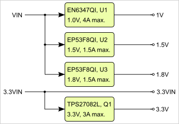
Power Distribution Diagram
| Page break |
|---|
Power-On Sequence
For highest efficiency of the on-board DC-DC regulators, it is recommended to use same 3.3V power source for both VIN and 3.3VIN power rails. Although VIN and 3.3VIN can be powered up in any order, it is recommended to power them up simultaneously.
...
| Note |
|---|
Initial state of the ON_1V0 and ON_1V8 signals and therefore also functionality of the NOSEQ signal depend on the System Controller CPLD firmware. |
| Page break |
|---|
Power Rails
B2B Name | B2B JM1 Pins | B2B JM2 Pins | Direction | Note |
|---|---|---|---|---|
| VIN | 1, 3, 5 | 2, 4, 6, 8 | Input | Supply voltage from carrier board. |
| 3.3VIN | 13, 15 | 91 | Input | Supply voltage from carrier board. JM2-91 is VREF_JTAG. |
| VCCIO35 | 9, 11 | - | Input | High range bank voltage from carrier board. |
| VCCIO33 | - | 5 | Input | High range bank voltage from carrier board. |
| VCCIO13 | - | 7, 9 | Input | High range bank voltage from carrier board. |
| VCCIO34 | - | 1, 3 | Input | High range bank voltage from carrier board. |
| VBAT_IN | 79 | - | Input | RTC battery-buffer supply voltage. |
| 3.3V | - | 10, 12 | Output | Internal 3.3V voltage level. |
| 1.8V | 39 | - | Output | Internal 1.8V voltage level. |
| 1.5V 1) | - | 19 | Output | Internal 1.5V voltage level. |
...
Overview
Content Tools