Page History
...
| USB PHY Pin | ZYNQ Pin | SC CPLD Pin | B2B Name | Notes |
|---|---|---|---|---|
| REFCLK | - | - | - | 52.000000 MHz reference clock from on-board oscillator (U14). |
| REFSEL0..2 | - | - | - | Reference clock frequency select, all set to GND selects 52.000000 MHz. |
| RESETB | - | B14, bank 1 | - | Active low reset. |
| CLKOUT | MIO36 | - | - | ULPI output clock mode. |
| DP, DM | - | OTG-D_P, OTG-D_N | USB data lines. | |
| CPEN | - | VBUS_V_EN | External USB power switch active high enable signal. | |
| VBUS | - | - | USB-VBUS | Connect to USB VBUS via a series of resistors, see reference schematicsschematic. |
| ID | - | - | OTG-ID | For A-device connect to the ground, for B-device leave floating. |
| SPK_L | - | M5, bank 2 | - | In USB audio mode a switch connects the DM pin to the SPK_L pin. |
| SPK_R | - | M8, bank 2 | - | In USB audio mode a switch connects the DP pin to the SPK_R pin. |
The schematics schematic for the USB connector and required components is different depending on the USB usage. USB standard A or B connectors can be used for host or device modes. A mini-USB connector can be used for USB device mode. A micro-USB connector can be used for device mode, OTG mode or host mode.
...
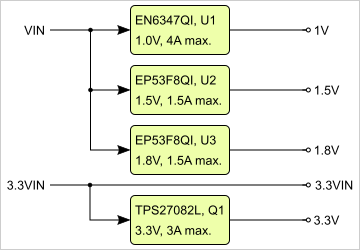
Power Distribution Diagram
| Note |
|---|
Current rating of Samtec LSHM Razor Beam B2B connectors is 2.0A per pin (2 adjacent pins powered). |
| Page break |
|---|
Power-On Sequence
...
1) In case of module variant of TE0720-03-L1IF which uses Xilinx Zynq XC7Z020-L1CLG484I chip with lower power consumption, power rails named 1.5V and VCCO_DDR_502 voltage is actually 1.35V. To achieve this, a resistor with different value is used for R4 (see schematics schematic of the TE0720-03-L1IF for more information).
Bank Voltages
Bank | Schematics Schematic Name | Voltage | Notes |
|---|---|---|---|
| 500 | 3.3V, VCCO_MIO0_500 | 3.3V | |
| 501 | 1.8V, VCCO_MIO1_501 | 1.8V | |
| 502 | 1.5V, VCCO_DDR_502 | 1.5V | |
| 0 Config | 3.3V | 3.3V | |
| 13 HR | VCCO13 | 1.2V to 3.3V | Supplied by the carrier board. |
| 33 HR | VCCIO33 | 1.2V to 3.3V | Supplied by the carrier board. |
| 34 HR | VCCIO34 | 1.2V to 3.3V | Supplied by the carrier board. |
| 35 HR | VCCIO35 | 1.2V to 3.3V | Supplied by the carrier board. |
...
Overview
Content Tools