Page History
...
- 5V power connector jack, J1
- Reset switch, S2
- USB type A receptacle, J7
- Micro SD card socket with Card Detect, J4
- 50 pin IDC male connector, J5
- 1000Base-T Gigabit RJ45 Ethernet MagJack, J3
- 1000Base-T Gigabit RJ45 Ethernet MagJack, J2
- JTAG/UART connector, JX1
- User DIP switch block, S1
- VCCO VCCIO voltage selection jumper block, J10 - J12
- External connector (VG96) placeholder, J6
- Samtec Razor Beam™ LSHM-150 B2B connector, JB1
- Samtec Razor Beam™ LSHM-150 B2B connector, JB2
- Samtec Razor Beam™ LSHM-130 B2B connector, JB3
...
JTAG access to the mounted 4 x 5 SoM is provided via 12-pin header JX1 and controlled by DIP switch S1-2 to select the device (Zynq-SoC, SC-CPLD) to programto program (see section 'DIP Switch S1').
This header has a 'XMOD FTDI JTAG Adapter'-compatible pin-assignment, so the XMOD-FT2232H adapter-board TE0790 can be used in conjunction with the carried board TE0706 Carrier Board to program the mounted SoM via USB interface.
...
The TE0706-02 is equipped with a Marvell Alaska 88E1512 Gigabit Ethernet PHY (U6) connected to the B2B connector JB3, which provides in conjunction with Gigabit Ethernet MagJack J2 a 1000Base-T Ethernet interface. The I/O Voltage is fixed at 1.8V. The reference clock input of the PHY is supplied by on-board 25MHz oscillator (U7).
PHY (U6) interface connectionspin assignment:
| PHY | B2B-pin | Notes |
|---|---|---|
| MDC/MDIO | JB3-49, JB3-51 | - |
| LED0 | - | Connected to Ethernet jack J2 LED0 (green). |
| LED1 | - | Connected to Ethernet jack J2 LED1 (green). |
| INT | JB3-33 | - |
| CONFIG | JB3-60 | - |
| RESET | JB3-53 | - |
| RGMII | JB3-37 - JB-44, JB3-47, JB3-57 - JB-59 | Reduced Gigabit Media Independent Interface. 12 pins. |
| SGMII | - | Serial Gigabit Media Independent Interface. Not connected. |
| MDI | - | Media Dependent Interface. Connected to Gigabit - Ethernet MagJack J2. |
RJ45 Gigabit Ethernet MagJack J3
...
| Info |
|---|
| Note: Pin OTG-ID is only assigned to USB 2.0 type B socket. |
DIP
...
Switch S1
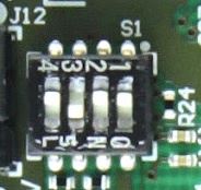
| Switch | Signal Name | ON | OFF | Notes |
|---|---|---|---|---|
| S1-1 | - | - | - | Not connected. |
| S1-2 | PROGMODE | JTAG enabled for programing mounted SoM's Zynq-SoC. | JTAG enabled for programing mounted SoM's SC-CPLD. | - |
| S1-3 | MODE | Drive SoM SC CPLD pin 'MODE' low. | Leave SoM SC CPLD pin 'MODE' open. | Boot mode configuration, if supported by SoM. (Depends also on SoM's SC-CPLD firmware). |
| S1-4 | EN1 | Drive SoM SC CPLD pin 'EN1' low. | Drive SoM SC CPLD pin 'EN1' high. | Usually used to enable/disable FPGA core-voltage supply. (Depends also on SoM's SC CPLD firmware). Note: Power-on sequence will be intermitted if S1-4 is set to OFF and if functionality is supported by SoM. |
...
| Power Input Pin | Max Current |
|---|---|
| VIN (power connector jack J1) | 3A |
The power-consumption of TE0706-02 in conjunction with different 4 x 5 SoMs under certain configurations are depending on the used model of the 4 x 5 SoM and the custom-made FPGA-design on this SoM. Please refer to the TRM of the mounted 4 x 5 SoM to get information about the typical power consumption.
...
Note: If supplying base-board supply-voltages by connector J6, the module's internal 3.3V voltage-level on pins 9 and 11 of B2B-connector JB2 has to be reached stable state.
| Note |
|---|
Take care of the VCCO voltage ranges of the particular PL IO-banks (HR, HP) of the mounted SoM, otherwise damages may occur to the FPGA. Therefore, refer to the TRM of the mounted SoM to get the specific information of the voltage ranges. It is recommended to set and measure the PL IO-bank supply-voltages before mounting of TE 4 x 5 module to avoid failures and damages to the functionality of the mounted SoM. |
| Info |
|---|
| Header J9 exposes the SoM's VBAT-pin to an accessible connector. Please refer to the SoM's documentation regarding the operation conditions of this pin. |
...
Overview
Content Tools