Page History
...
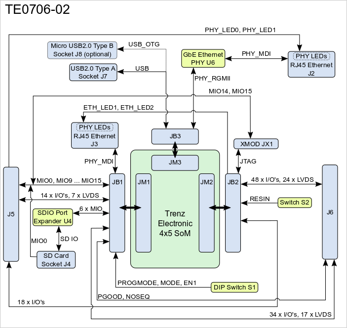
- VG96 backplane connector (mounting holes and solder pads, J6) and 50-pin IDC male connector socket (J5) to access FPGA bank's IO-pins
- SDIO port expander with voltage-level translation
- Micro SD card socket, routed to B2B-connector JB1
- USB type A connector (OTG mode), routed to B2B-connecor JB3
- 1 x user-push button S2, routed to RESIN-pin on B2B-connector JB2. By default it is configured as system reset button.
- 1 x RJ45 Gigabit Ethernet MagJack J3, PHY_MDI interface routed to B2B-connector JB1.
- 1 x Marvell Alaska 88E1512 Ethernet PHY, routed to B2B-connector JB3 and accessible via RJ45 Gigabit Ethernet MagJack J2
- Barrel jack for 5 V Power Supply input
- 4 A High-Efficiency Power SoC DC-DC Step-Down Converter (Enpirion EN6347) for 3.3 V Power Supply
- Trenz 4 x 5 Module Socket (3 x Samtec LSHM series connectors)
- JTAG/UART-pins on 12-pin header JX1, routed to B2B-connector JB2
- user configurable DIP switch S1 to set System Controller CPLD signals on SoM
- 3 x VCCIO selection jumper J10, J11 and J12 to set SoM's bank voltages
Block Diagram
Main Components
...
Overview
Content Tools