Page History
...
DIP-Switch S1
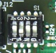
Figure 2: User DIP-Switch S1
| Switch | Signal Name | ON | OFF | Notes |
|---|---|---|---|---|
| S1-1 | - | - | - | Not connected. |
| S1-2 | PROGMODE | JTAG enabled for programing mounted SoM's Zynq-SoC. | JTAG enabled for programing mounted SoM's SC-CPLD. | - |
| S1-3 | MODE | Drive SoM SC CPLD pin 'MODE' low. | Leave SoM SC CPLD pin 'MODE' open. | Boot mode configuration, if supported by SoM. (Depends also on SoM's SC-CPLD firmware). |
| S1-4 | EN1 | Drive SoM SC CPLD pin 'EN1' low. | Drive SoM SC CPLD pin 'EN1' high. | Usually used to enable/disable FPGA core-voltage supply. (Depends also on SoM's SC CPLD firmware). Note: Power-on sequence will be intermitted if S1-4 is set to OFF and if functionality is supported by SoM. |
...
It is not allowed to feed any voltage to any external I/O pin before there is no power indication on M3.3VOUT pins. Presence of 3.3V on B2B JB2 connector pins 9 and 11 indicates that module is properly powered up and ready. The 1.8V voltage-level on base-board for supplying PL I/O bank supply-voltages will be powered up after the module's 3.3V voltage-level has reached stable state and M3.3VOUT is available on the B2B-connector JB2, pins 9 and 11.
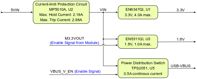
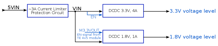
Figure 3: TE0706-02 power-up sequence diagram.
...
Overview
Content Tools