Page History
| Scroll Ignore |
|---|
Download PDF Version of this Document. |
| Scroll pdf ignore | ||||
|---|---|---|---|---|
Table of Contents
|
Overview
| Scroll Only (inline) |
|---|
Refer to https://shop.trenz-electronic.de/de/Download/?path=Trenz_Electronic/carrier_boards/TEBB0714 for downloadable version of this manual and additional technical documentation of the product. |
The Trenz Electronic TEBB0714 is a base-board for test- and evaluation-purposes, especially for the Multi-gigabit transceiver units of the TE0714 module. Although this base-board is dedicated to the TE0714 module, it is also compatible with other Trenz Electronic 4 x 5 cm SoMs. See page "4 x 5 cm carriers" to get information about the SoMs supported by the TEBB0714 base-board.
This base-board provides also soldering-pads as place-holders for pin-headers as option to get access to the PL-IO-banks of the mounted SoM.
Key Features
- SFP+ connector (Enhanced small form-factor pluggable), supports data transmission rates up to 10 Gbit/s
- 4 Hirose Ultra small SMT coaxial connectors, supports data transmission rates up to 6 Gbit/s
- TE 4 x 5 cm SoM programable by JTAG header (JX1)
- 2 x user LEDs routed to IO-pins of the SoM
- Soldering-pads J17 and J20 for optional pin headers for access to SoM's IO-bank-pins, usable as LVDS-pairs
- Soldering-pads J3 and J4 for optional pin headers for access to further interfaces and IO's of the SoM
Block Diagram
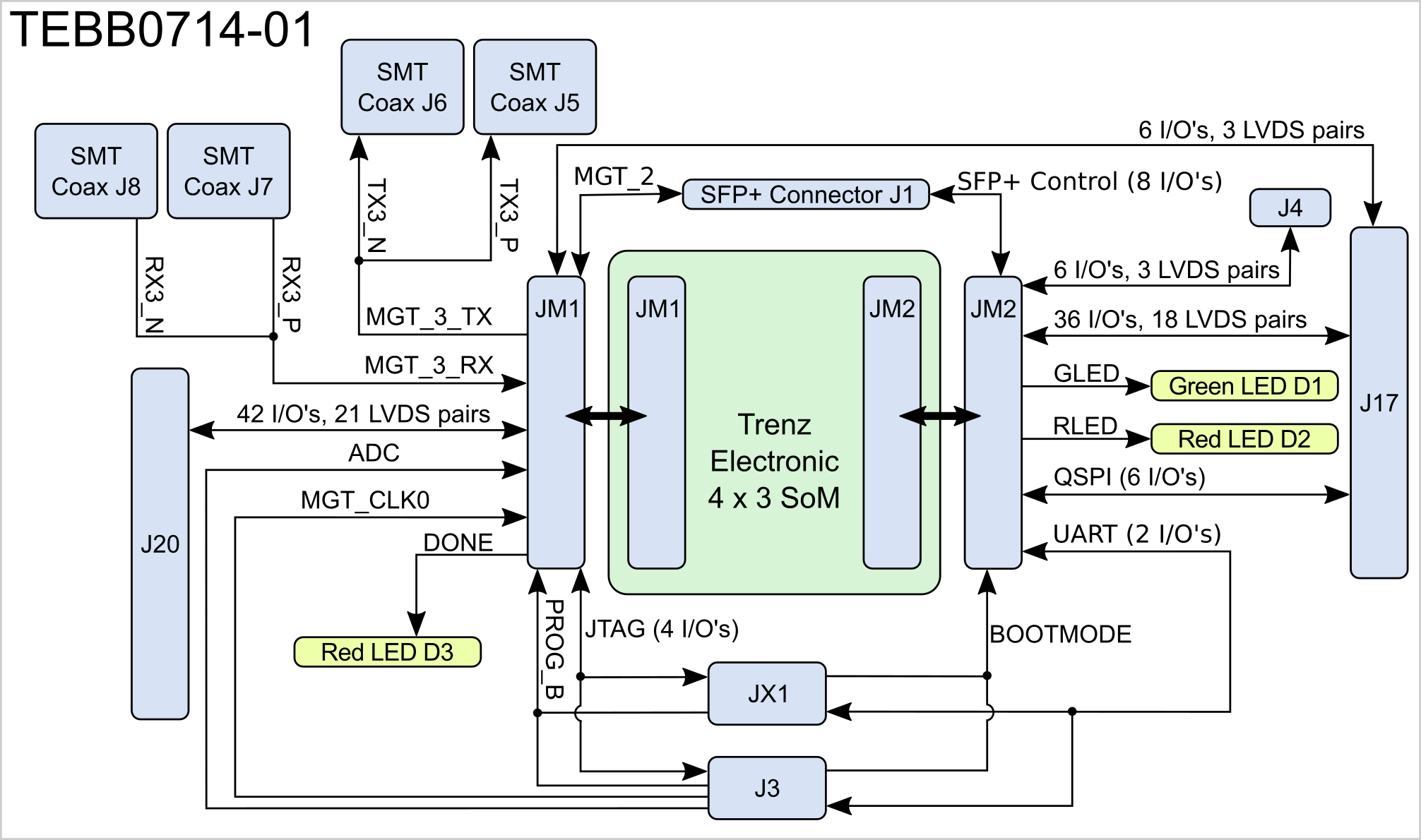
Figure 1: TEBB0714 -01 Block Diagram
Main Components
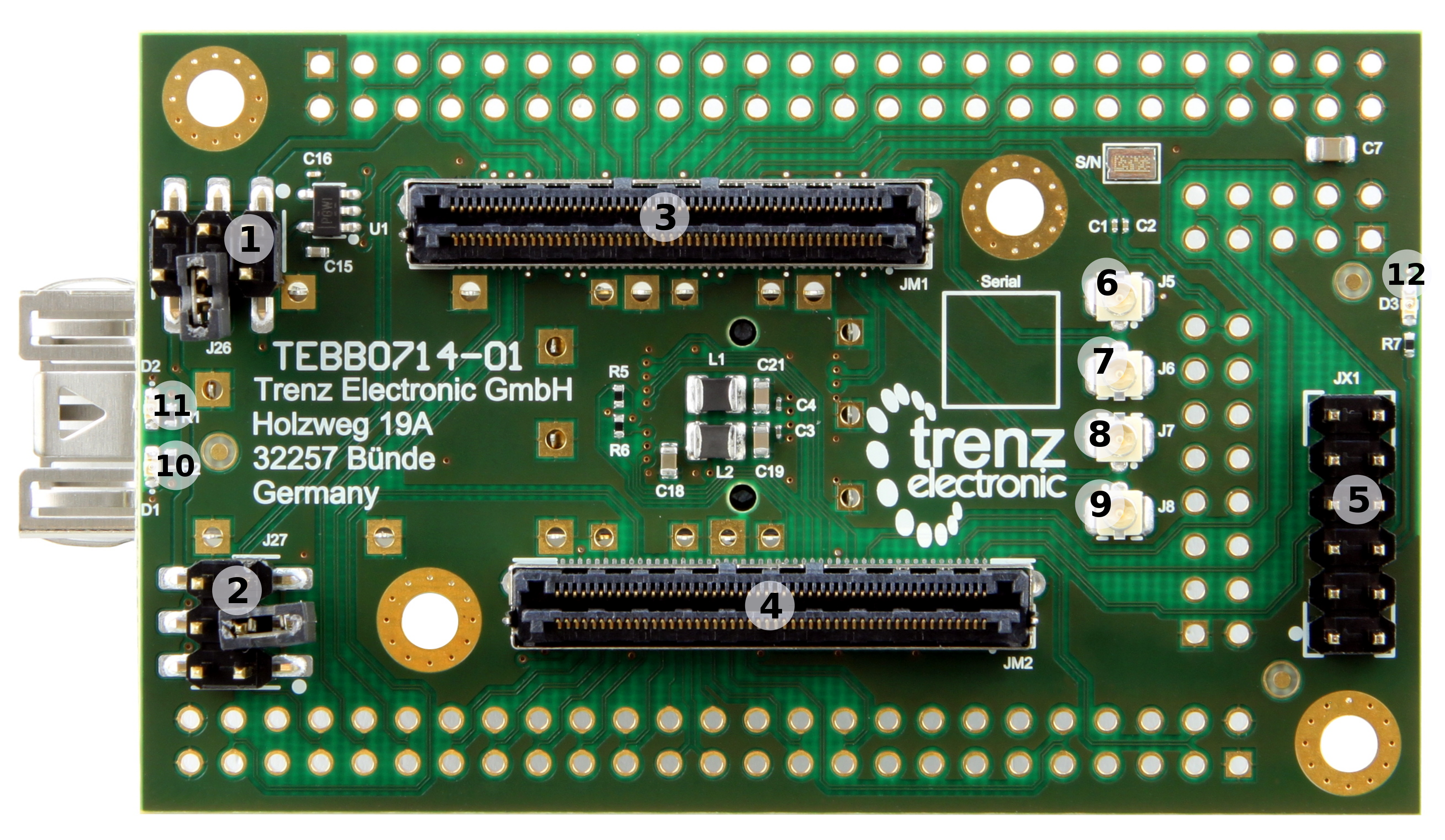
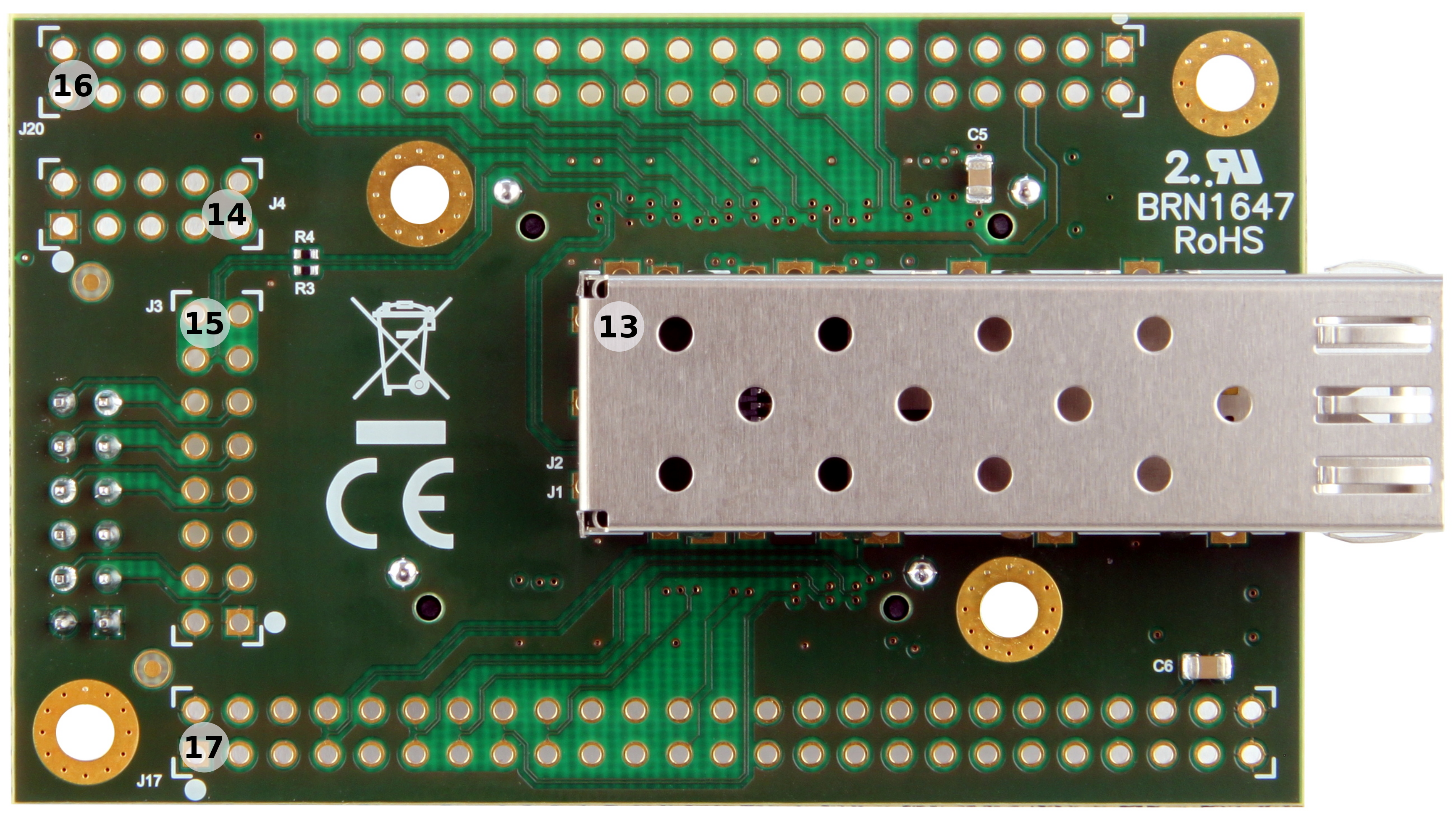
Figure 2: 4 x 5 cm SoM carrier board TEBB0714-01
TEBB0714 -01:
- 6-pin header J26 for selecting Bank34 VCCIO voltage
- 6-pin header J27 for selecting XMOD/JTAG reference voltage
- Samtec Razor Beam™ LSHM-150 B2B connector JM1
- Samtec Razor Beam™ LSHM-150 B2B connector JM2
- JTAG/UART header JX1 ('XMOD FTDI JTAG Adapter'-compatible pin-assignment)
- Ultra small SMT coaxial connector J5
- Ultra small SMT coaxial connector J6
- Ultra small SMT coaxial connector J7
- Ultra small SMT coaxial connector J8
- User LED D1 (green)
- User LED D2 (red)
- LED D3 (red) indicating 'Programming DONE'-signal from module's FPGA
- SFP+ Connector J1
- 10-pin header soldering-pads J4 for access to SoM's PL IO-banks (LVDS-pairs possible)
- 16-pin header soldering-pads J3, JTAG/UART header ('XMOD FTDI JTAG Adapter'-compatible pin-assignment)
- 50-pin header soldering-pads J20 for access to SoM's PL IO-banks (LVDS-pairs possible)
- 50-pin header soldering-pads J17 for access to SoM's PL IO-banks (LVDS-pairs possible)
Interfaces and Pins
SFP+ Connector
The TEBB0714 carrier board there provides a SFP+ connector J1 (board-rev. 01: Molex 74441-0001). The connector is embedded into a SFP cage J2 (board-rev. 01: Molex 74737-0009).
The RX-/TX-data-lanes are connected to B2B-connector JM1, the control-lines are connected to pins on B2B-connector JM2.
On this SFP+ connector, MGT-lane 2 is accessible at mounted 4 x 5 SoM TE0714.
The pin-assignment of the SFP connector is in detail as fellows:
| SFP+ Pin | Pin Schematic Name | B2B Connector | Note |
|---|---|---|---|
| Transmit Data + (pin 18) | MGT_TX2_P | JM1-14 | - |
| Transmit Data - (pin 19) | MGT_TX2_N | JM1-16 | - |
| Receive Data + (pin 13) | MGT_RX2_P | JM1-7 | - |
| Receive Data - (pin 12) | MGT_RX2_N | JM1-9 | - |
| Transmit Fault (pin 2) | SFP0_TX_FAULT | JM2-42 | - |
| Transmit disable (pin 3) | SFP0_TX_DIS | JM2-44 | - |
| MOD-DEF2 (pin 4) | SFP0_SDA | JM2-46 | 3.3V pull-up, (usable as I²C-SDA) |
| MOD-DEF1 (pin 5) | SFP0_SCL | JM2-48 | 3.3V pull-up, (usable as I²C-SCL) |
| MOD-DEF0 (pin 6) | SFP0_M0DEF0 | JM2-40 | - |
| RS0 (pin 7) | SFP0_RS0 | JM2-38 | - |
| LOS (pin 8) | SFP0_LOS | JM2-34 | - |
| RS1 (pin 9) | SFP0_RS1 | JM2-32 | - |
Table 1: SFP+ connector pin-assignment
Ultra Small SMT Coaxial Connectors
4 HIROSE Ultra Small Surface Mount Coaxial Connectors are on the base-board available for access to the MGT-lange 3 of the SoM with data transmission rates up to 6 Gbit/s. The connectors have the manufacturer designation 'U.FL-R-SMT-1', mating hight: 2.4 mm.
Each conductor of the RX- and TX-LVDS-pair is routed to one coaxial connector:
| Connector Designator | Connected to | B2B Connector |
|---|---|---|
| J5 | MGT_TX3_P | JM1-8 |
| J6 | MGT_TX3_N | JM1-10 |
| J7 | MGT_RX3_P | JM1-1 |
| J8 | MGT_RX3_N | JM1-3 |
Table 2: Pin-assignment of the coaxial connectors
JTAG/UART Interface
The JTAG interface of the mounted 4 x 5 SoM can be accessed via header JX1 or J3, which has two additional pins (15,16) as LVDS-pair to supply the mounted 4 x 5 SoM with an external reference clock-signal.
The headers JX1 and J3 have a 'XMOD FTDI JTAG Adapter'-compatible pin-assignment, so in use with the XMOD-FT2232H adapter-board TE0790 the mounted SoM can be programmed via USB interface.
| JX1-pin | Pin Schematic Name | B2B Connector | J3-pin | Pin Schematic Name | B2B Connector | |
|---|---|---|---|---|---|---|
| C (pin 4) | TCK | JM1-90 | 4 | TCK | JM1-90 | |
| D (pin 8) | TDO | JM1-88 | 8 | TDO | JM1-88 | |
| F (pin 10) | TDI | JM1-86 | 10 | TDI | JM1-86 | |
| H (pin 12) | TMS | JM1-92 | 12 | TMS | JM1-92 | |
| A (pin 3) | B14_L25 (usable as UART RX/TX-line) | JM2-97 | 3 | B14_L25 | JM2-97 (usable as UART RX/TX-line) | |
| B (pin 7) | B14_L0 (usable as UART RX/TX-line) | JM2-99 | 7 | B14_L0 | JM2-99 (usable as UART RX/TX-line) | |
| E (pin 9) | BOOTMODE | JM2-100 | 9 | BOOTMODE | JM2-100 | |
| G (pin 11) | PROG_B | JM1-94 | 11 | PROG_B | JM1-94 | |
| - | - | - | 13 | XADC_P | JM1-25 (ADC_P, decoupling capacitator 100 nF) | |
| - | - | - | 14 | XADC_N | JM1-27 (ADC_N, decoupling capacitator 100 nF) | |
| - | - | - | 15 | CLK0_P | JM1-2 (MGT_CLK0_P, 1KΩ serial resistor) | |
| - | - | - | 16 | CLK0_N | JM1-4 (MGT_CLK0_N, 1KΩ serial resistor) |
Table 3: JTAG/UART header JX1 / J3 pin-assignment
On both interfaces (JX1, J3), the pins with the net-names B14_L25 and B14_L0 are available as user IO's which could be used as UART-interface for example.
LEDs
Three LEDs are present on the TEBB0714 base-board with following functionality:
| LED Designator | Color | Pin Schematic Name | B2B Connector | Indicating |
|---|---|---|---|---|
| D1 | green | GLED | JM2-26 | available to user |
| D2 | red | RLED | JM2-24 | available to user |
| D3 | red | DONE | JM1-96 | FPGA-modul programmed properly |
Table 4: LED's functionality
Place Holders for Optional Pin-headers
The TEBB0714 base-board has place-holders with solder-pads to mount optional pin-headers capable to access the PL IO-bank pins of the mounted 4 x 5 SoM. With mounted pin-headers SoM's IO's are available to the user, a large quantity of these IO's are also usable as LVDS-pairs. This pin-headers provide also VCCIO voltages to operate the IO's properly.
Following table gives a summary of the optional pin-headers of the base-board:
Connector Designator | Pin-header Layout | Count of IO's | Count of LVDS-pairs | Available VCCIO's | Interfaces |
|---|---|---|---|---|---|
| J4 | 2-row 10-pin | 6 | 3 | 3.3V 3.3V_OUT (from mounted module) | - |
| J17 | 2-row 50-pin | 42 (Bank 14) | 18 | 3.3V V_CFG (internal module's VCCIO: 3.3V or 1.8V, depending on configuration) | QSPI (6 IO's) |
| J20 | 2-row 50-pin | 42 (Bank 34) | 21 | 3.3V VCCIO34 (selectable: 1.8V, 2.5V, 3.3V_OUT) | - |
| J3 | 2-row 16-pin | 12 | 2 | 3.3V V_CFG (internal module's VCCIO: 3.3V or 1.8V, depending on configuration) | JTAG (4 IO's) UART (2 IO's) ADC (1 LVDS-pair) Reference clock input MGT-CLK0 (1 LVDS-pair) |
Table 5: Summary of optional pin-headers
Power
Power Supply
Power supply with minimum current capability of 3A at 3.3V for system startup is recommended.
The on-board voltages of the carrier board will be powered up with an external power-supply with nominal voltage of 3.3V.
The external power-supply can be connected to the board by the following pins:
| Connector | 3.3V pin | GND Pin |
|---|---|---|
| JX1 | JX1-5 | JX1-1, JX1-2 |
| J3 | J3-5 | J3-1, J3-2 |
| J4 | J4-5 | J4-1, J4-2 |
| J20 | J20-5, J20-46 | J20-1 , J20-2 , J20-49 , J20-50 |
| J17 | J17-5, J17-46 | J17-1 , J17-2 , J17-49 , J17-50 |
Table 6: Connector-pins capable for external 3.3V power-supply
Power-On Sequence
The PL IO-bank supply-voltages 1.8V, 2.5V and 3.3V will be powerd up after the mounted module's 3.3V voltage level has reached stable state on B2B-connector pin JM1-83, meaning that all on-module voltages have become stable and module is properly powered up.
Note: The supply-voltages have low current dropout.
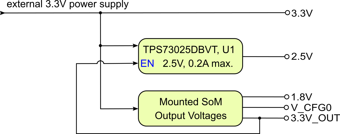
Figure 3: Power-On sequence diagram
Configuring VCCIO
On the TEBB0714 carrier board different VCCIO configurations can be chosen by the jumper J26 and J27.
The purpose of the jumper of the carrier board will be explained in the following sections.
Summary of VCCIO-configuration
On the TEBB0714 carrier board the PL IO-bank's supply voltage VCCIO34 is selectable between the supply-voltages 1.8V, 2.5V and 3.3V via jumper J26. The supply voltage VCCIO15 is routed on board to the pin '3.3V_OUT', hence it is fixed to 3.3V.
Following table describes how to configure the base-board supply-voltage VCCIO34 by jumper J26:
Base-board Supply Voltage VCCIO34 | Jumper J26 |
|---|---|
| 1.8V | J26:1-2 |
| 2.5V | J26:3-4 |
| 3.3V | J26: 5-6 |
Table 6: Configuration of base-board supply-voltages via jumpers.
By jumper J27 the reference voltage of the JTAG/UART header JX1 (pin 6 VIO) can be selected:
Reference VCCIO JTAG/UART Header V_CFG | Jumper J27 |
|---|---|
| 1.8V | J27:1-2 |
| V_CGF0 (internal module's VCCIO: 3.3V or 1.8V, depending on configuration) | J27:3-4 |
| 3.3V_OUT | J27: 5-6 |
Table 7: Configuration of reference VCCIO JTAG/UART header.
Jumper-Notification: 'Jx: 1-2' means pins 1 and 2 are connected, 'Jx: 3-4' means pins 3 and 4 are connected, and so on. Other pins are left open.
| Note |
|---|
Take care of the VCCO voltage ranges of the particular PL IO-banks (HR, HP) of the mounted SoM, otherwise damages may occur to the FPGA. Therefore, refer to the TRM of the mounted SoM to get the specific information of the voltage ranges. It is recommended to set and measure the PL IO-bank supply-voltages before mounting of TE 4x5 module to avoid failures and damages to the functionality of the mounted SoM. |
Technical Specifications
Absolute Maximum Ratings
| Parameter | Min | Max | Units | Notes |
|---|---|---|---|---|
Vin supply voltage | 3.135 | 3.465 | V | 3.3V supply-voltage ± 5% |
Storage Temperature | -55 | 105 | °C | Molex 74441-0001 Product Specification |
Recommended Operating Conditions
| Parameter | Min | Max | Units | Notes |
|---|---|---|---|---|
| Vin supply voltage | 3.135 | 3.465 | V | - |
Physical Dimensions
Board size: PCB 46 mm × 75 mm. Notice that some parts the are hanging slightly over the edge of the PCB like the the SFP+ connector, which determine the total physical dimensions of the carrier board. Please download the assembly diagram for exact numbers.
Mating height of the module with standard connectors: 8mm
PCB thickness: ca. 1.65mm
Highest part on the PCB is the SFP+ connector, which has an approximately 11.3 mm overall hight. Please download the step model for exact numbers.
The dimensions are given in mm and mil (milli inch).
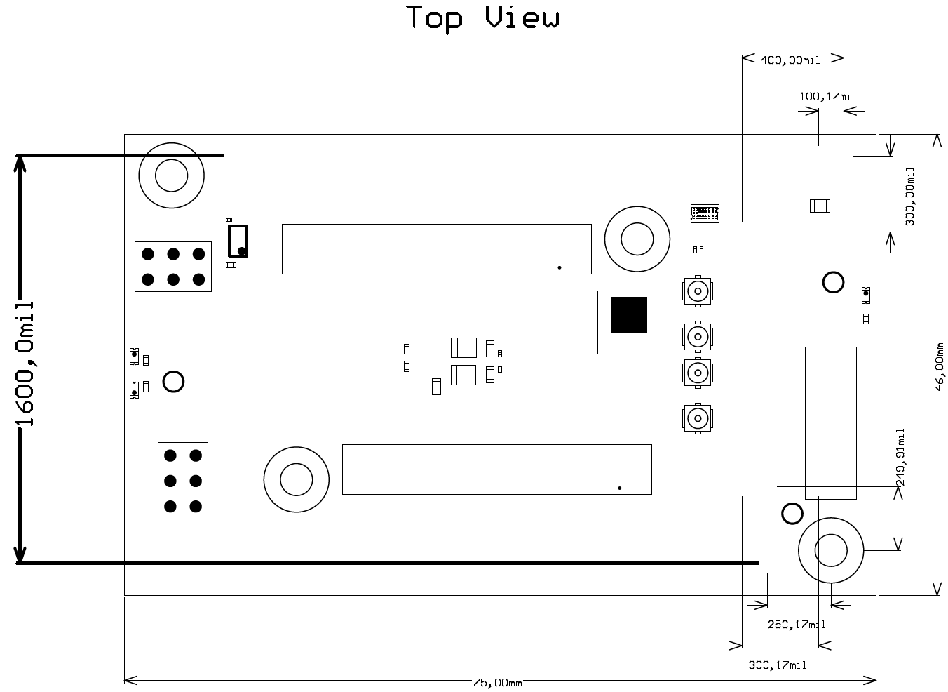
Figure 4: Physical Dimensions of the TEBB0714-01 carrier board
Operating Temperature Ranges
Commercial grade: 0°C to +70°C.
Board operating temperature range depends also on customer design and cooling solution. Please contact us for options.
Weight
ca. 25 g - Plain board
Document Change History
| Date | Revision | Authors | Description |
|---|---|---|---|
| 2017-06-27 | Ali Naseri | current TRM for TEBB0714-01 | |
| 2017-01-30 | 0.1 | Ali Naseri | Initial document |
Hardware Revision History
| Date | Revision | Notes | PCN | Documentation link |
|---|---|---|---|---|
| - | 01 |
|
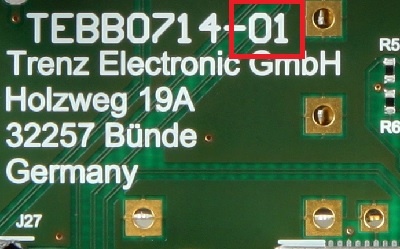
Figure 5: Hardware revision Number
Hardware revision number is printed on the PCB board next to the model number separated by the dash.
Disclaimer
| Include Page | ||||
|---|---|---|---|---|
|
Overview
Content Tools