Page History
...
| HTML |
|---|
<!-- Template Revision 1.5 --> |
| Scroll Only (inline) |
|---|
Online version of this manual and other related documents can be found at https://wiki.trenz-electronic.de/display/PD/SC-CPLD-Firmware |
| Scroll pdf ignore | ||||
|---|---|---|---|---|
Table of contents
|
...
Firmware for PCB CPLD with designator U6. Second CPLD Device in Chain: LCMX02-256HC
| Info |
|---|
2 Firmware variants with swapped external reset input and output direction are available. See 105689936 section of this document. Firmware (SC729_03_default_teb0729_02_plus.jed) for J2-89 as external reset output and J2-91 as external reset input will be used as default firmware. |
| Warning |
|---|
Watchdog do not work correctly on all modules with Firmware released before 2017.08.22. Please update Firmware on CPLD. For questions, write to Trenz Electronic support. |
Feature Summary
- Boot Mode
- JTAG connection
- Power Management
- ...Watchdog Management
Firmware Revision and supported PCB Revision
...
| Name / opt. VHD Name | Direction | Pin | Description |
|---|---|---|---|
| BOARD_STAT | out | 23 | STATUS to B2B |
| BOOT_MODE1 | in | 28 | Boot Mode Pin from B2B |
| BOOT_MODE2 | in | 27 | Boot Mode Pin from B2B |
| BOOT1 | out | 13 | Boot Mode Pin to FPGA (MIO4) |
| BOOT2 | out | 12 | Boot Mode Pin to FPGA (MIO5) |
| EN_3V3 | out | 25 | Enable 3.3V Switch |
| F_TCK | out | 8 | JTAG to FPGA |
| F_TDI | out | 9 | JTAG to FPGA |
| F_TDO | in | 11 | JTAG from FPGA |
| F_TMS | out | 10 | JTAG to FPGA |
| FPGA_IO | in | 5 | USR Status output from FPGA |
| JTAGSEL | --- | 26 | Enable JTAG access to CPLD for Firmware update (zero: JTAG routed to FPGA, one: CPLD access) |
| nRST | inout | 16 | External Reset. Direction Firmware depends, see Watchdog section |
| nRST_IN | inout | 4 | External Reset. Direction Firmware depends, see Watchdog section |
| PS_POR_B | in | 14 | Reset from Watchdog to FPGA |
| TCK | in | 30 | JTAG from B2B |
| TDI | in | 32 | JTAG from B2B |
| TDO | out | 1 | JTAG to B2B |
| TMS | in | 29 | JTAG from B2B |
| WD_EN | in | 21 | Watchdog PL I/O |
| WD_HIT | in | 20 | Watchdog PL I/O |
| WDI | out | 17 |
| Watchdog trigger to external Watchdog IC |
Functional Description
JTAG
JTAG signals routed directly through the CPLD to FPGA. Access between CPLD and FPGA can be multiplexed via JTAGSEL (logical one for CPLD, logical zero for FPGA) on J2-111.
Power
3.3V (EN_3V3) is enabled on power up.
Boot Mode
Boot Mode Pins routed through the CPLD. MIO2 and MIO3 are connected to GND via resistor.
| Pin | FPGA IO |
|---|---|
| BOOT_MODE1 (BOOT1) | MIO4 |
| BOOT_MODE2 (BOOT2) | MIO5 |
| BOOT1 | BOOT2 | Boot Mode |
|---|---|---|
| 0 | 0 | JTAG |
| 0 | 1 | QSPI |
| 1 | 0 | not supported |
| 1 | 1 | SD |
Watchdog
Watchdog (TPS3310K33DMVR) is controlled by B2B IO, CPLD, Zynq IO or 1V power supply voltage.
TPS3310K33DMVR WDI Timing Requirenments:
| Time-out period | tT(OUT) | at WDI | min 0,55s, typ 1,1s, max 1,65s |
| Pulse width | tw | at WDI | 300ns |
Firmware Variants:
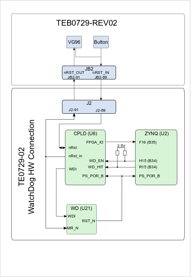 Figure1: Firmware (SC729_03_teb0729_02_org.jed) for TEB0729 without HW modification,
| 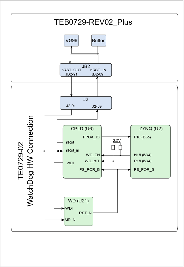 Figure2: Firmware (SC729_03_default_teb0729_02_plus.jed) for TEB0729 with HW modification,
|
B2B Control:
2 Variant available,depends on carrier board connection, see Figure 1 and 2. The swapped signals and nRST_IN pulse limitation on variant 1 are the only difference between this two variants.
Variant 1 (Figure 1, SC729_rev02org.jed):
| IOs | B2B | Direction | Description |
|---|---|---|---|
| nRST | J2-89 | inout | Main Reset to module |
| nRST_IN | J2-91 | out | Main reset to carrier and PS_POR_B for approx. 1,9 us. |
Variant 2 (Figure 2, SC729_rev02plus.jed):
| IOs | B2B | Direction | Description |
|---|---|---|---|
| nRST | J2-89 | out | Main reset to carrier and PS_POR_B |
| nRST_IN | J2-91 | inout | Main Reset to module |
1V Power supply:
Reset PS, if 1V drop down. Connected on PCB, controlled by WD SENSE pin.
CPLD Control:
CPLD controlled WD on power up until FPGA takes control via WE_EN and WD_HIT input. CPLD WDI pulse frequency is set to approx. 1ms (Pulse width tw(CPLD)=507us )
nRST_IN is set to GND on power up for short time periode
FPGA Control:
WD_HIT pulse will be forwarded to WDI pin, if WE_EN is high and min 16 WD_HIT from FPGA was detected. WD_EN can't be disabled until module was reboot.
WDI max. pulse width: tw(FPGA)<tT(out)- tw(CPLD)
Status / GPIO
BOARD_STAT is used as WD restart indicator and as user IO.
| Modus | Condition |
|---|---|
| Slow Blink | If PS_POR_B is low and appr. 16s after PS_POR_B goes up |
| FPGA_IO | User defined, appr. 16s after PS_POR_B goes up and as long as PS_POR_B is high |
Info: On TEB0729, signal is connected to XMOD LED.
Appx. A: Change History and Legal Notices
Revision Changes
CPLD REV03 to REV04
- Remove possibility to disable WD again via FPGA
CPLD REV02 to REV03
- Add power up Watchdog main reset from CPLD
CPLD REV01 to REV02
- Bugfix for TE0729-REV02 Watchdog support
- Add 2 Variants for TEB0729-REV02 and TE0729-REV02_MOD support
- Change Pin FGPA_IO direction
- Change Pin BOARD_STAT output configuration
Document Change History
To get content of older revision got to "Change History" of this page and select older document revision number.
...
| Date | Document Revision | CPLD Firmware Revision | Supported PCB Revision | Authors | Description | |||||||||||||||||||||||||||||
|---|---|---|---|---|---|---|---|---|---|---|---|---|---|---|---|---|---|---|---|---|---|---|---|---|---|---|---|---|---|---|---|---|---|---|
|
| REV02REV04 | REV02/REV02plus |
|
| |||||||||||||||||||||||||||||
| 2017-10-25 | v.17 | REV03 | REV02/REV02plus | John Hartfiel |
| |||||||||||||||||||||||||||||
| 2017-08-31 | v.14 | REV02 | REV02/REV02plus | John Hartfiel | ||||||||||||||||||||||||||||||
| 2017-08-23 | v.13 | REV02 | REV02/REV02plus | John Hartfiel |
| |||||||||||||||||||||||||||||
| 2017-06-07 | REV02 | REV02/REV02plus |
|
| ||||||||||||||||||||||||||||||
| All |
|
Legal Notices
| Include Page | ||||
|---|---|---|---|---|
|
Overview
Content Tools