Page History
...
| HTML |
|---|
<!-- Template Revision 1.5 --> |
| Scroll Only (inline) |
|---|
Online version of this manual and other related documents can be found at https://wiki.trenz-electronic.de/display/PD/SC-CPLD-Firmware |
| Scroll pdf ignore | ||||
|---|---|---|---|---|
Table of contents
|
...
| Info |
|---|
2 Firmware variants with swapped external reset input and output direction are available. See Watchdog 105689936 section of this document. Firmware (SC729_03_default_teb0729_02_plus.jed) for J2-89 as external reset output and J2-91 as external reset input will be used as default firmware. |
| Warning |
|---|
Watchdog do not work correctly on all modules with Firmware released before 2017.08.22. Please update Firmware on CPLD. For questions, write to Trenz Electronic support. |
Feature Summary
- Boot Mode
- JTAG connection
- Power Management
- Watchdog Management
...
| Name / opt. VHD Name | Direction | Pin | Description |
|---|---|---|---|
| BOARD_STAT | out | 23 | STATUS to B2B |
| BOOT_MODE1 | in | 28 | Boot Mode Pin from B2B |
| BOOT_MODE2 | in | 27 | Boot Mode Pin from B2B |
| BOOT1 | out | 13 | Boot Mode Pin to FPGA (MIO4) |
| BOOT2 | out | 12 | Boot Mode Pin to FPGA (MIO5) |
| EN_3V3 | out | 25 | Enable 3.3V Switch |
| F_TCK | out | 8 | JTAG to FPGA |
| F_TDI | out | 9 | JTAG to FPGA |
| F_TDO | in | 11 | JTAG from FPGA |
| F_TMS | out | 10 | JTAG to FPGA |
| FPGA_IO | in | 5 | USR Status output from FPGA |
| JTAGSEL | --- | 26 | Enable JTAG access to CPLD for Firmware update (zero: JTAG routed to FPGA, one: CPLD access) |
| nRST | inout | 16 | External Reset. Direction Firmware depends, see Watchdog section |
| nRST_IN | inout | 4 | External Reset. Direction Firmware depends, see Watchdog section |
| PS_POR_B | in | 14 | Reset from Watchdog to FPGA |
| TCK | in | 30 | JTAG from B2B |
| TDI | in | 32 | JTAG from B2B |
| TDO | out | 1 | JTAG to B2B |
| TMS | in | 29 | JTAG from B2B |
| WD_EN | in | 21 | Watchdog PL I/O |
| WD_HIT | in | 20 | Watchdog PL I/O |
| WDI | out | 17 | Watchdog trigger to external Watchdog IC |
...
Functional Description
JTAG
...
Power
3.3V (EN_3V3) is enabled on power up.
Boot Mode
Boot Mode Pins routed through the CPLD. MIO2 and MIO3 are connected to GND via resistor.
| Pin | FPGA IO |
|---|---|
| BOOT_MODE1 (BOOT1 (BMODE1) | MIO4 |
| BOOT_MODE2 (BOOT2 (BMODE2) | MIO5 |
| BOOT1 | BOOT2 | Boot Mode |
|---|---|---|
| 0 | 0 | JTAG |
| 0 | 1 | QSPI |
| 1 | 0 | not supported |
| 1 | 1 | SD |
...
TPS3310K33DMVR WDI Timing Requirenments:
| Time-out period | tT(OUT) | at WDI | min 0,55s, typ 1,1s, max 1,65s |
| Pulse width | tw | at WDI | 300ns |
Firmware Variants:
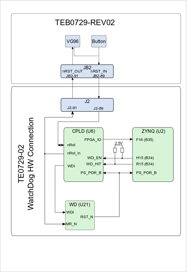 Figure1: Firmware (SC729_03_teb0729_02_org.jed) for TEB0729 without HW modification,
| 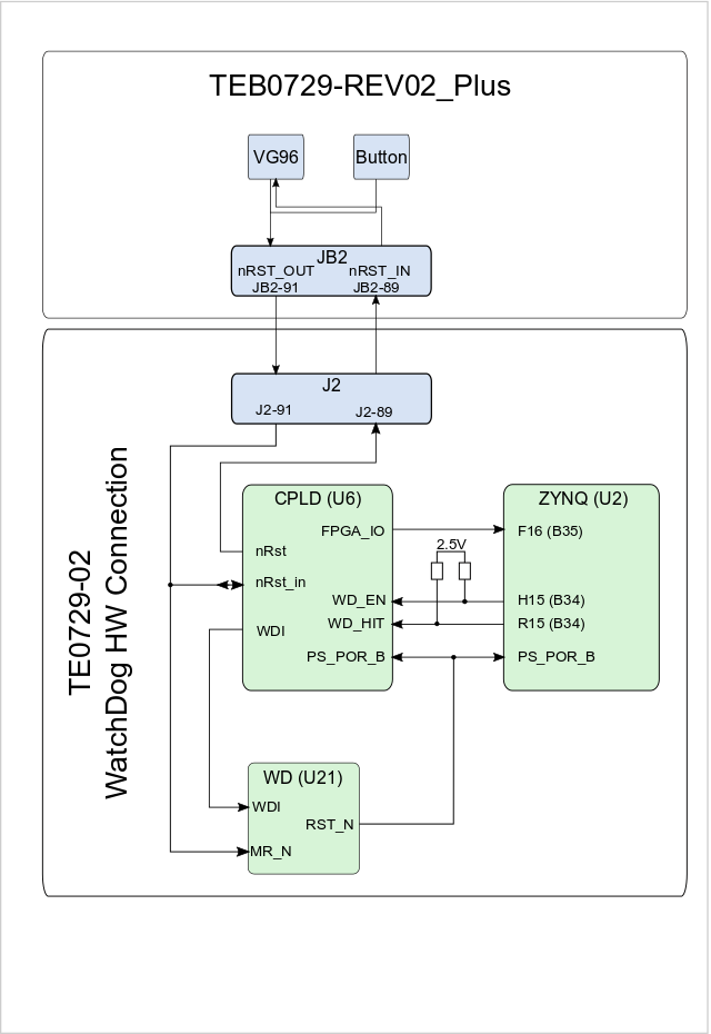 Figure2: Firmware (SC729_03_default_teb0729_02_plus.jed) for TEB0729 with HW modification,
|
...
B2B Control:
2 Variant available,depends on carrier board connection, see Figure 1 and 2. The swapped signals and nRST_IN pulse limitation on variant 1 are the only difference between this two variants.
Variant 1 (Figure 1, SC729_rev02org.jed):
| IOs | B2B | Direction | Description |
|---|---|---|---|
| nRST | J2-89 | ininout | Main Reset to module |
| nRST_IN | J2-91 | out | Main reset to carrier and PS_POR_B for approx. 1,9 us. |
Variant 2 (Figure 2, SC729_rev02plus.jed):
| IOs | B2B | Direction | Description |
|---|---|---|---|
| nRST | J2-89 | out | Main reset to carrier and PS_POR_B |
| nRST_IN | J2-91 | ininout | Main Reset to module |
1V Power supply:
...
CPLD controlled WD on power up until FPGA takes control via WE_EN and WD_HIT input. CPLD WDI pulse frequency is set to approx. 1ms (Pulse width tw(CPLD)=507us )
nRST_IN is set to GND on power up for short time periode
FPGA Control:
WD_HIT pulse will be forwarded to WDI pin, if WE_EN is high and min 16 WD_HIT from FPGA was detected. To disable FPGA Control, set WD_EN to lowcan't be disabled until module was reboot.
WDI max. pulse width: tw(FPGA)<tT(out)- tw(CPLD)
...
| Modus | Condition |
|---|---|
| Slow Blink | If PS_POR_B is low and appr. 30s long 16s after PS_POR_B goes up |
| FPGA_IO | User defined, appr. 30s long 16s after PS_POR_B goes up and as long as PS_POR_B is high |
...
Info: On TEB0729, signal is connected to XMOD LED.
Appx. A: Change History and Legal Notices
Revision Changes
CPLD REV03 to REV04
- Remove possibility to disable WD again via FPGA
CPLD REV02 to REV03
- Add power up Watchdog main reset from CPLD
CPLD REV01 to REV02
- Bugfix for TE0729-REV02 Watchdog support
- Add 2 Variants for TEB0729-REV02 and TE0729-REV02_MOD support
- Change Pin FGPA_IO direction
- Change Pin BOARD_STAT output configuration
...
| Date | Document Revision | CPLD Firmware Revision | Supported PCB Revision | Authors | Description | |||||||||||||||||||||||||||
|---|---|---|---|---|---|---|---|---|---|---|---|---|---|---|---|---|---|---|---|---|---|---|---|---|---|---|---|---|---|---|---|---|
|
| REV02REV04 | REV02/REV02plus |
|
| |||||||||||||||||||||||||||
| 2017-10-25 | v.17 | REV03 | REV02/REV02plus | John Hartfiel |
| |||||||||||||||||||||||||||
| 2017-08-31 | v.14 | REV02 | REV02/REV02plus | John Hartfiel | ||||||||||||||||||||||||||||
| 2017-08-23 | v.13 | REV02 | REV02/REV02plus | John Hartfiel |
| |||||||||||||||||||||||||||
| 2017-06-07 | REV02 | REV02/REV02plus |
|
| ||||||||||||||||||||||||||||
| All |
|
Legal Notices
| Include Page | ||||
|---|---|---|---|---|
|
Overview
Content Tools