Page History
| HTML |
|---|
<!--
Template Revision 1.3 beta
(HTML comment will not display, it's not needed to remove them. For Template/Skeleton changes, increase Template Revision number. So we can check faster, if the TRM style is up to date)
--> |
| Scroll Ignore |
|---|
Download PDF version of this document. |
| Scroll pdf ignore | |
|---|---|
Table of Contents
|
Overview
| Scroll Only (inline) |
|---|
Refer to "https://shop.trenz-electronic.de/en/Download/?path=Trenz_Electronic/TE0808" for downloadable version of this manual and the rest of available documentation. |
The Trenz Electronic TE0808 is an industrial-grade MPSoC SoM integrating a Xilinx Zynq UltraScale+, max. 8 GByte DDR4 SDRAM with 64-Bit width databus connection, max. 512 MByte Flash memory for configuration and operation, 20 Gigabit transceivers and powerful switch-mode power supplies for all on-board voltages. A large number of configurable I/O's is provided via rugged high-speed stacking connections.
All this in a compact 5.2 x 7.6 cm form factor, at the most competitive price.
| Note |
|---|
Important Information for TE0808 boards which are equipped with ES1 or ES2 silicon: Erratas and functional restrictions may exist, please check Xilinx documentation and contact your local Xilinx FAE for restrictions. |
...
Download PDF version of this document.
| Scroll pdf ignore | |
|---|---|
Table of Contents
|
Overview
| Scroll Only (inline) |
|---|
Refer to "https://shop.trenz-electronic.de/en/Download/?path=Trenz_Electronic/TE0808" for downloadable version of this manual and the rest of available documentation. |
The Trenz Electronic TE0808 is an industrial-grade MPSoC UltraSoM integrating a Xilinx Zynq UltraScale+, max. 8 GByte DDR4 SDRAM with 64-Bit width databus connection, max. 512 MByte Flash memory for configuration and operation, 20 Gigabit transceivers, and powerful switch-mode power supplies for all on-board voltages. A large number of configurable I/O's is provided via rugged high-speed stacking connections.
| Note |
|---|
Current TE0808 boards are equipped with ES1 silicon. Erratas and functional restrictions may exist, please check Xilinx documentation and contact your local Xilinx FAE for restrictions. |
Block Diagram
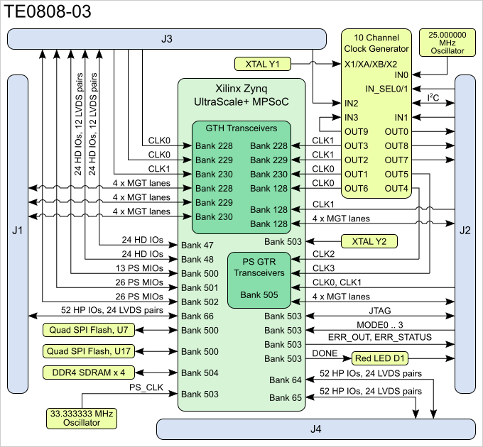
Figure 1: TE0808-03 Block Diagram
Main Components
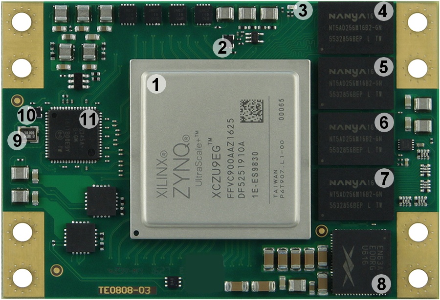

Figure 2: TE0808-03 MPSoC module
- Xilinx ZYNQ UltraScale+ XCZU9EG MPSoC, U1
- Low-power programmable oscillator @ 33.333333 MHz (PS_CLK), U32
- Red LED (DONE), D1
- 256Mx16 DDR4-2400 SDRAM, U12
- 256Mx16 DDR4-2400 SDRAM, U9
- 256Mx16 DDR4-2400 SDRAM, U2
- 256Mx16 DDR4-2400 SDRAM, U3
- 12A PowerSoC DCDC converter, U4
- Quartz crystal, Y1
- Low-power programmable oscillator @ 25.000000 MHz (IN0 for U5), U25
- 10-channel programmable clock generator, U5
- Ultra fine 0.50 mm pitch, Razor Beam™ LP Slim Terminal Strip with 160 contacts, J4
- Ultra fine 0.50 mm pitch, Razor Beam™ LP Slim Terminal Strip with 160 contacts, J2
- Ultra fine 0.50 mm pitch, Razor Beam™ LP Slim Terminal Strip with 160 contacts, J3
- Ultra fine 0.50 mm pitch, Razor Beam™ LP Slim Terminal Strip with 160 contacts, J1
- Quartz crystal, Y2
- 256 Mbit serial NOR Flash memory, U7
- 256 Mbit serial NOR Flash memory, U17
Key Features
- MPSoC: ZYNQ UltraScale+ ZU9EG 900 pin package
- Memory
- 64-Bit DDR4, 8 GByte maximum
- Dual SPI boot Flash in parallel, 512 MByte maximum - User I/O
- 65 x MIO, 48 x HD (all), 156 x HP (3 banks)
- Serial transceiver: 4 x GTR + 16 x GTH
- Transceiver clocks inputs and outputs
- PLL clock generator inputs and outputs - Size: 52 x 76 mm, 3 mm mounting holes for skyline heat spreader
- B2B connectors: 4 x 160 pin
- Si5345 - 10 output PLL
- All power supplies on board, single 3.3V power source required
- 14 on-board DCDC regulators and 13 LDOs
- LP, FP, PL separately controlled power domains - Support for all boot modes (except NAND) and scenarios
- Support for any combination of PS connected peripherals
Initial Delivery State
...
Content
...
Notes
...
SPI Flash main array
...
Not programmed
...
eFUSE Security
...
Not programmed
...
Block Diagram

Figure 1: TE0808-04 Block Diagram
Main Components
Figure 2: TE0808 MPSoC module
- Xilinx ZYNQ UltraScale+ XCZU9EG MPSoC, U1
- Low-power programmable oscillator @ 33.333333 MHz (PS_CLK), U32
- Red LED (DONE), D1
- 256Mx16 DDR4-2400 SDRAM, U12
- 256Mx16 DDR4-2400 SDRAM, U9
- 256Mx16 DDR4-2400 SDRAM, U2
- 256Mx16 DDR4-2400 SDRAM, U3
- 12A PowerSoC DCDC converter, U4
- Quartz crystal, Y1
- Low-power programmable oscillator @ 25.000000 MHz (IN0 for U5), U25
- 10-channel programmable PLL clock generator, U5
- Ultra fine 0.50 mm pitch, Razor Beam™ LP Slim Terminal Strip with 160 contacts, J4
- Ultra fine 0.50 mm pitch, Razor Beam™ LP Slim Terminal Strip with 160 contacts, J2
- Ultra fine 0.50 mm pitch, Razor Beam™ LP Slim Terminal Strip with 160 contacts, J3
- Ultra fine 0.50 mm pitch, Razor Beam™ LP Slim Terminal Strip with 160 contacts, J1
- Quartz crystal, Y2
- 256 Mbit serial NOR Flash memory, U7
- 256 Mbit serial NOR Flash memory, U17
Initial Delivery State
| Storage device name | Content | Notes |
|---|---|---|
SPI Flash main array | Not programmed | - |
eFUSE Security | Not programmed | - |
| Si5345A programmable PLL NVM OTP | Not programmed | - |
Table 1: Initial Delivery State of the flash memories
Signals, Interfaces and Pins
Board to Board (B2B) connectors
The TE0808 MPSoC SoM has four Board to Board (B2B) connectors with 160 contacts per connector.
Each connector has a specific arrangement of the signal pins, which are grouped together in categories related to their functionalities and to their belonging to particular units of the Zynq Ultrascale+ MPSoC like I/O-banks, interfaces and Gigabit transceivers
or to the on-board peripherals.
Following table lists the I/O-bank signals, which are routed from the MPSoC's PL and PS banks as LVDS pairs or single ended I/O's to the B2B connectors.
| Bank | Type | B2B Connector | Schematic Names / Connector Pins | I/O Signal Count | LVDS Pairs Count | VCCO Bank Voltage | Notes |
|---|---|---|---|---|---|---|---|
| 47 | HD | J3 | B47_L1_P ... B47_L12_P |
Table 1: Initial Delivery State of the flash memories
Signals, Interfaces and Pins
Board to Board (B2B) connectors
The TE0808 MPSoC UltraSoM has four Board to Board (B2B) connectors with 160 contacts per connector.
Each connector has a specific arrangement of the signal-pins, which are grouped together in categories related to their functionalities and to their belonging to particular units of the Zynq Ultrascale+ MPSoC like I/O-banks, interfaces and Gigabit transceivers
or to the on-board peripheral ICs of the SoM.
Following table lists the I/O-bank signals, which are routed from the MPSoC's PL and PS banks as LVDS-pairs or single ended I/O's to the B2B connectors.
| Bank | Type | B2B Connector | Schematic names / Connector pins | I/O signal count | LVDS-pairs count | VCCO bank voltage | Notes |
|---|---|---|---|---|---|---|---|
| 47 | HD | J3 | B47_L1_P ... B47_L12_P | 24 I/O's | 12 | VCCO47 | VCCO max. 3.3V |
| 48 | HD | J3 | B48_L1_P ... B48_L12_P | 24 I/O's | 12 | VCCO47VCCO48 | VCCO max. 3.3V |
| 6448 | HPHD | J4J3 | B64B48_L1_P ... B64B48_L24L12_P | 48 24 I/O's | 2412 | VCCO48VCCO64 | VCCO max. 13.8V3V |
| 64 | HP | J4 | B65B64_L1_P ... B65B64_L24_P | 48 I/O's | 24 | VCCO64VCCO65 | VCCO max. 1.8V |
| 64 | HP | J4 | B_64_T0 ... B_64_T3 | 4 I/O's | - | VCCO64 | VCCO max. 1.8V only single-ended I/O's |
| 65 | HP | J4 | BB65_65L1_T0 P ... BB65_65L24_P | 48 I/O's | 24 | VCCO65 | VCCO max. 1.8V |
| 65 | HP | J4 | B_65_T0 ... B_65_T3 | 4 I/O's | - | VCCO65 | VCCO max. 1.8V only single-ended I/O's |
| 66 | HP | J1 | B66_L1_P ... B66_L24_P | 48 I/O's | 24 | VCCO66 | VCCO max. 1.8V |
| 66 | HP | J1 | B_66_T0 ... B_66_T3 | 4 I/O's | - | VCCO66 | VCCO max. 1.8V |
| 500 | PSMIOMIO | J3 | MIO13 ... MIO25 | 13 I/O's | - | PS_1V8- | user configurable I/O's on B2B |
| 501 | PSMIOMIO | J3 | MIO26 ... MIO51 | 26 I/O's | - | PS_1V8- | user configurable I/O's on B2B |
| 502 | PSMIOMIO | J3 | MIO52 ... MIO77 | 26 I/O's | - | PS_1V8- | user configurable I/O's on B2B |
Table 2: B2B connector pin-outs of available PL and PS banks of the TE0808-03 SoM04 SoM
All MIO banks are powered from on-module DC-DC power rail. All PL I/O Banks have separate VCCO pins in the B2B connectors, valid VCCO should be supplied from the baseboard.
For detailed information about the B2B pin-out, please refer to the Pin-out table.
MGT lanes
The configuration of the I/O's MIO13 - MIO77 are depending on the base-board peripherals connected to these pins.
MGT Lanes
The B2B connector J1 and J2 provide also access to the MGT-banks of the Zynq UltrascaleThe B2B connector J1 and J2 provide also access to the MGT-banks of the Zynq Ultrascale+ MPSoC. There are 20 high-speed data lanes (Xilinx GTH / GTR transceiver) available composed as differential signaling pairs for both directions (RX/TX).
The MGT-banks have also clock input-pins which are exposed to the B2B connectors J2 and J3. Following MGT-lanes are available on the B2B connectors:
| Bank | Type | B2B Connector | count Count of MGT lanesLanes | Schematic names Names / Connector pinsPins | MGT bankBank's reference clock inputs (LVDS-pairs)Reference Clock Inputs |
|---|---|---|---|---|---|
| 228 | GTH | J1 | 4 GTH lanes | B228_RX3_P, B228_RX3_N, pins J1-27, J1-29 B228_RX2_P, B228_RX2_N, pins J1-33, J1-35 B228_RX1_P, B228_RX1_N, pins J1-39, J1-41 B228_RX0_P, B228_RX0_N, pins J1-45, J1-47 | 1 reference clock signal (B228_CLK0) from B2B connector 1 reference clock signal (B228_CLK1) from programmable |
| 229 | GTH | J1 | 4 GTH lanes | B229_RX3_P, B229_RX3_N, pins J1-27, J1-29 B229_RX2_P, B229_RX2_N, pins J1-33, J1-35 B229_RX1_P, B229_RX1_N, pins J1-39, J1-41 B229_RX0_P, B229_RX0_N, pins J1-45, J1-47 | 1 reference clock signal (B229_CLK0) from B2B connector 1 reference clock signal (B229_CLK1) from programmable |
| 230 | GTH | J1 | 4 GTH lanes | B230_RX3_P, B230_RX3_N, pins J1-3, J1-5 B230_RX2_P, B230_RX2_N, pins J1-9, J1-11 B230_RX1_P, B230_RX1_N, pins J1-15, J1-17 B230_RX0_P, B230_RX0_N, pins J1-21, J1-23 | 1 reference clock signal (B230_CLK1) from B2B connector 1 reference clock signal (B230_CLK0) from programmable |
| 128 | GTH | J2 | 4 GTH lanes | B128_RX3_N, B128_RX3_P, pins J2-28, J2-30 B128_RX2_N, B128_RX2_P, pins J2-34, J2-36 B128_RX1_N, B128_RX1_P, pins J2-40, J2-42 B128_RX0_N, B128_RX0_P, pins J2-46, J2-48 | 1 reference clock signal (B128_CLK1) from B2B connector 1 reference clock signal (B128_CLK0) from programmable |
| 505 | GTR | J2 | 4 GTR lanes | B505_RX3_N, B505_RX3_P, pins J2-52, J2-54 B505_RX2_N, B505_RX2_P, pins J2-58, J2-60 B505_RX1_N, B505_RX1_P, pins J2-64, J2-66 B505_RX0_N, B505_RX0_P, pins J2-70, J2-72 | 2 reference clock signals (B505_CLK0, B505_CLK1) from B2B connector 2 reference clock signal (B505_CLK2, B505_CLK3) from programmable |
Table 3: B2B connector pin-outs of available MGT-lanes of the MPSoC
JTAG Interface
JTAG access is provided through the MPSoC's PS configuration bank 503 with bank voltage 'PS_1V8'.
| JTAG Signal | B2B Connector pinPin |
|---|---|
| TCK | J2-120 |
| TDI | J2-122 |
| TDO | J2-124 |
| TMS | J2-126 |
Table 4: B2B connector pin-out of JTAG interface
Configuration
...
Bank Control Signals
The Xilinx Zynq Ultrascale+ MPSoC's PS configuration bank 503 control signal pins are accessible through B2B-connector J2.
For further information about the particular control signals and how to use and evaluate them, refer to the Xilinx Zynq Ultrascale+ MPSoC TRM and UltraScale Architecture Configuration - User Guide.
| Signal | B2B Connector Pin | Function |
|---|---|---|
| Signal | B2B Connector pin | Function |
| DONE | J2-116 | PL configuration completed |
| PROG_B | J2-100 | PL configuration reset signal |
| INIT_B | J2-98 | PS is initialized after a power-on reset |
| SRST_B | J2-96 | System reset |
| MODE0 ... MODE3 | J2-109/J2-107/J2-105/J2-103 | 4-bit boot mode pins For further information about the boot-modes refer to the Xilinx Zynq Ultrascale+ MPSoC TRM |
| ERR_STATUS / ERR_OUT | J2-86 / J2-88 | ERR_OUT signal is asserted for accidental loss of ERR_STATUS indicates a secure lockdown state |
| PUDC_B | J2-127 | Pull-up during configuration (pulled-up to 'PL_1V8') |
Table 5: B2B connector pin-out of MPSoC's PS configuration bank
Analog Input
The Xilinx Zynq Ultrascale+ MPSoC provides input-pins differential pairs for differential analog input values. The pins are exposed to B2B-connector J2.
| Signal | B2B Connector pinPin | Function |
|---|---|---|
| V_P, V_N | J2-113, J2-115 | System Monitor |
| DX_P, DX_N | J2-119, J2-121 | Temperature-sensing diode pins |
Table 6: B2B connector pin-out of analog input pins
Quad
...
SPI
...
Interface
Quad SPI Flash memory ICs The TE0808-03 SoM is equipped with two Serial Flash Memory with up to 512 Mbyte storage capacity each. The flash memory ICs with the schematic designators U7 and U17 are connected to bank 500 (PSMIO) of the Zynq MPSoC module via QSPI interface, enabling a 8-Bit width databus connection.
Following table shows the mapping of the MIO-pins to the flash memory ICs.
...
Chip-select (low-active)
...
Chip-select (low-active)
...
Table 7: Flash memory QSPI-interface
DDR4 SDRAM
The TE0808-03 UltraSoM is equipped with with four DDR4-2400 SDRAM modules with up to 8 Gbyte memory density. The SDRAM modules are connected to the Zynq MPSoC's PS DDR-controller (bank 504) with a 64-bit databus width.
LEDs
TE0808 has one red LED (D1) which reflects MPSoC's 'DONE' signal. This LED goes ON when power has been applied to the module and stays ON until MPSoC's programmable logic is configured properly.
Clocking
Programmable Clock Generator
Following table illustrates on-board Si5345A programmable clock multiplier chip inputs and outputs:
...
Table 8: Programmable PLL clock generator input/output
The Si5345A programmable clock generator's control interface pins are exposed to B2B connector J2. For further information refer to the Si5345A data sheet.
...
Device Reset (low-active)
...
I²C interface, needed extern pull-ups.
I²C address in current configuration: 1101010b
the Zynq PS QSPI0 interface via PS MIO bank 500, pins MIO0 ... MIO5 and MIO7 ... MIO12.
| MIO | Signal Schematic Name | U7 Pin | MIO | Signal Schematic Name | U17 Pin | |
|---|---|---|---|---|---|---|
| 0 | SPI Flash-SCK/M4 | B2 | 7 | SPI Flash-SCK | C2 | |
| 1 | SPI Flash-DQ1/M1 | D2 | 8 | SPI Flash-DQ0/M0 | D3 | |
| 2 | SPI Flash-DQ2/M2 | C4 | 9 | SPI Flash-DQ1/M1 | D2 | |
| 3 | SPI Flash-DQ3/M3 | D4 | 10 | SPI Flash-DQ2/M2 | C4 | |
| 4 | SPI Flash-DQ0/M0 | D3 | 11 | SPI Flash-DQ3/M3 | D4 | |
| 5 | SPI Flash-SCK | C2 | 12 | SPI Flash-SCK/M4 | B2 |
Table 7: MIO-pin assignment of the Quad SPI Flash memory ICs
Boot Process
Full access to B2B connector. For Functional details see ug1085 - Zynq ultrascale TRM (Boot Modes Section).
| Boot Mode Pin | B2B Pin |
|---|---|
| PS_MODE0 | J2-109 |
| PS_MODE1 | J2-107 |
| PS_MODE2 | J2-105 |
| PS_MODE3 | J2-103 |
On-board Peripherals
Flash
The TE0808 SoM can be configured with max. 512 MByte Flash memory for configuration and operation.
| Name | IC | Designator | PS7 | MIO | Notes |
|---|---|---|---|---|---|
| SPI Flash | N25Q256A11E1240E | U7 | QSPI0 | MIO0 ... MIO5 | dual parallel booting possible, 32 MByte memory per Flash IC at standard configuration |
| SPI Flash | N25Q256A11E1240E | U17 | QSPI0 | MIO7 ... MIO12 | as above |
Table 8: Peripherals connected to the PS MIO-pins
DDR4 SDRAM
The TE0808-04 SoM is equipped with with four DDR4-2400 SDRAM modules with up to 8 GByte memory density. The SDRAM modules are connected to the Zynq MPSoC's PS DDR-controller (bank 504) with a 64-bit databus width.
Refer to the Xilinx Zynq Ultrascale+ data sheet DS925 to get information, if the specific package of the Zynq Ultrascale+ MPSoC equipped on module supports the maximum data transmission rate of 2400 MByte/s.
Programmable PLL Clock Generator
Following table illustrates on-board Si5345A programmable clock multiplier chip inputs and outputs:
| Input | Connected to | Frequency | Notes |
|---|---|---|---|
| IN0 | On-board Oscillator (U25) | 25.000000 MHz | - |
| IN1 | B2B Connector pins J2-3, J2-1 (differential pair) | User | AC decoupling required on base |
| IN2 | B2B Connector pins J3-66, J3-68 (differential pair) | User | AC decoupling required on base |
| IN3 | OUT9 | User | Loop-back from OUT9 |
| Output | Connected to | Frequency | Notes |
| OUT0 | B2B Connector pins J2-3, J2-1 (differential pair) | User | Default off |
| OUT1 | B230 CLK0 | User | Default off |
| OUT2 | B229 CLK1 | User | Default off |
| OUT3 | B228 CLK1 | User | Default off |
| OUT4 | B505 CLK2 | User | Default off |
| OUT5 | B505 CLK3 | User | Default off |
| OUT6 | B128 CLK0 | User | Default off |
| OUT7 | B2B Connector pins J2-7, J2-9 (differential pair) | User | Default off |
| OUT8 | B2B Connector pins J2-13, J2-15 (differential pair) | User | Default off |
| OUT9 | IN3 (Loop-back) | User | Default off |
| XA/XB | Quartz (Y1) | 50.000 MHz | - |
Table 9: Programmable PLL clock generator input/output
The Si5345A programmable clock generator's control interface pins are exposed to B2B connector J2. For further information refer to the Si5345A data sheet.
| Signal | B2B Connector Pin | Function |
|---|---|---|
| PLL_FINC | J2-81 | Frequency Increment |
| PLL_LOLN | J2-85 | Loss Of Lock (low-active) |
| PLL_SEL0 / PLL_SEL1 | J2-93 / J2-87 | Manual Input Switching |
| PLL_FDEC | J2-94 | Frequency Decrement |
| PLL_RST | J2-59 | Device Reset (low-active) |
| PLL_SCL / PLL_SDA | J2-90 / J2-92 | I²C interface, extern pull-ups needed for SCL- / SDA-line. I²C address in current configuration: 1101000b |
Table 10: B2B connector pin-out of Si5345A programmable clock generator
| Note |
|---|
Si5345 OTP ROM is not programmed by default at delivery, so it is customers responsibility to either configure Si5345 during FSBL or then use SiLabs programmer and burn the OTP ROM with customer fixed clock setup. |
Si5345 OTP can only be programmed two times, as different user configurations may required different setup TE0808 is normally shipped with blank OTP.
For more information Si5345 at SiLabs.
Oscillators
The TE0808-04 SoM is equipped with two on-board oscillators to provide the Zynq's MPSoC's PS configuration bank 503 with reference clock-signals.
| Clock | Frequency | Bank 503 Pin | Connected to |
|---|---|---|---|
| PS_CLK | 33.333333 MHz | P20 | MEMS Oscillator, U32 |
| PS_PAD (RTC) | 32.768 kHz | R22/R23 | Quartz crystal, Y2 |
Table 11: Reference clock-signals to PS configuration bank 503
On-board LEDs
LED | Color | Connected to | Description and Notes |
|---|---|---|---|
| D1 | red | DONE signal (PS Configuration Bank 503) | This LED goes ON when power has been applied to the module and stays ON until MPSoC's programmable logic is configured properly. |
Table 12: LED's description
Power and Power-On Sequence
Power Consumption
The maximum power consumption of a module mainly depends on the design which is running on the FPGA.
Xilinx provide a power estimator excel sheets to calculate power consumption. It's also possible to evaluate the power consumption of the developed design with Vivado. See also Trenz Electronic Wiki FAQ.
| Power Input Pin | Typical Current |
|---|---|
| DCDCIN | TBD* |
| LP_DCDC | TBD* |
| PL_DCIN | TBD* |
| PS_BATT | TBD* |
Table 13: Maximum current of power supplies. *to be determined soon with reference design setup.
Power supply with minimum current capability of 3A for system startup is recommended. For the lowest power consumption and highest efficiency of on board DC/DC regulators it is recommended to powering the module from one single 3.3V supply. Except 'PS_BATT', all input power supplies have a nominal value of 3.3V. Although the input power supplies can be powered up in any order, it is recommended to power them up simultaneously.
The TE0808 module equipped with the Xilinx Zynq Ultrascale+ MPSoC delivers a heterogeneous multi-processing system with integrated programmable logic and independently operable elements and is designed to meet embedded system power management requirement by advanced power management features. This features allow to offset the power and heat constraints against overall performance and operational efficiency.
This features allowing highly flexible power management are achieved by establishing Power Domains for power isolation. The Zynq Ultrascale+ MPSoC has multiple power domains, whereby each power domain requires its own particular extern DCDC converters.
The Processing System contains three Power Domains:
- Battery Power Domain (BBRAM and RTC)
- Full-Power Domain (Application Processing Unit, DDR Controller, Graphics Processing Unit and High-Speed Connectivity)
- Low-Power Domain (Real-Time Processing Unit, Security and Configuration Unit, Platform Management Unit, System Monitor and General Connectivity)
The fourth Power Domain is for the Programmable Logic (PL). If individual Power Domain control is not required, power rails can be shared between domains.
On the TE0808-04 SoM, following Power Domains can be powered up individually with power rails available on the B2B connectors:
- Full-Power Domain, supplied by power rail 'DCDCIN'
- Low-Power Domain, supplied by power rail 'LP_DCDC'
- Programmable Logic, supplied by power rail 'PL_DCIN'
- Battery Power Domain, supplied by power rail 'PS_BATT'
Each Power Domain has its own "Enabling"- and "Power Good"-signals. The power rail 'GT_DCDC' is necessary for generating the voltages for the Multi Gigabit Transceiver units of the Zynq Ultrascale+ MPSoC.
Power Distribution Dependencies
The power rails 'DCDCIN', 'LP_DCDC', 'PL_DCIN', 'PS_BATT' have to be powered up on the assigned pins of the B2B connectors as listed on the section "Power Rails". Except 'PS_BATT' (see section "Recommended Operation Conditions"), all power-rails can be powered up, with 3.3V power sources, also shared, if Power Domain control is not required.
There are following dependencies how the initial voltages of the power rails on the B2B connectors are distributed to the on-board DCDC converters, which power up further DCDC converters and the particular on-board voltages:
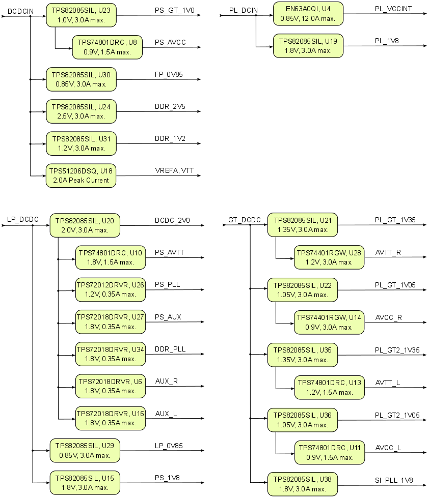
Figure 3: Power Distribution Diagram
| Note |
|---|
Current rating of Samtec Razor Beam™ LSHM B2B connectors is 2.0A per pin (2 adjacent pins powered). |
Power-On Sequence Diagram
The TE0808 SoM meets the recommended criteria to power up the Xilinx Zynq Ultrascale+ MPSoC properly by keeping a specific sequence
Table 9: B2B connector pin-out of Si5345A programmable clock generator
The TE0808-03 SoM is equipped with two on-board oscillators to provide the Zynq's MPSoC's PS configuration bank 503 with reference clock-signals.
...
Table 10: Reference clock-signals to PS configuration bank 503
Power and Power-On Sequence
Power supply with minimum current capability of 3A for system startup is recommended. For the lowest power consumption and highest efficiency of on board DC/DC regulators it is recommended to powering the module from one single 3.3V supply. All input power supplies have a nominal value of 3.3V. Although the input power supplies can be powered up in any order, it is recommended to power them up simultaneously.
The TE0808-03 module with the Xilinx Zynq Ultrascale+ MPSoC delivers a heterogeneous multi-processing system with integrated programmable logic and independently operable elements and is designed to meet embedded system power management requirement by advanced power management features. This features allow to offset the power and heat constraints against overall performance and operational efficiency.
This features allowing highly flexible power management are achieved by establishing Power Domains for power isolation. The Zynq Ultrascale+ MPSoC has multiple power domains, whereby each power domain requires its particular extern DCDC converters.
The Processing System contains three Power Domains:
- Battery Power Domain (BBRAM and RTC)
- Full-Power Domain (Application Processing Unit, DDR Controller, Graphics Processing Unit and High-Speed Connectivity)
- Low-Power Domain (Real-Time Processing Unit, Security and Configuration Unit, Platform Management Unit, System Monitor and General Connectivity)
The fourth Power Domain is for the Programmable Logic (PL). If individual Power Domain control is not required, power rails can be shared between domains.
On the TE0808-03 SoM, following Power Domains can be powered up individually with power rails available on the B2B connectors:
- Full-Power Domain, supplied by power rail 'DCDCIN'
- Low-Power Domain, supplied by power rail 'LP_DCDC'
- Programmable Logic, supplied by power rail 'PL_DCIN'
- Battery Power Domain, supplied by power rail 'PS_BATT'
Each Power Domain has its own "Enabling"- and "Power Good"-signal. The power rail 'GT_DCDC' is necessary for generating the supply voltages for the high speed Gigabit Transceivers units of the Zynq Ultrascale+ MPSoC.
Power-On Sequence utilizing DCDC control signals
To power up the TE0808-03 SoM properly, a specific sequence must be kept of enabling the on-board DCDC converters dedicated to the particular Power Domains and powering up the on-board voltages.
The first activated Power Domain is the Low-Power Domain. Therefore, the power rail 'LP_DCDC' have to be powered up and the Enable-signal 'EN_LPD' (pin J2-108, 7V max.) have to be asserted. The resulting Power-Good-Signal 'LP_GOOD' (pin J2-106) will go high after the voltages of the Low-Power Domain are properly powered up.
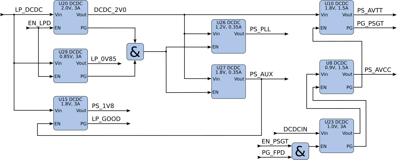
Figure 3: Low-Power Domain
The second activated Power Domain is the Programmable Logic. Therefore, the power rail 'PL_DCIN' have to be powered up and the Enable-signal 'EN_PL' (pin J2-101) have to be asserted by pulling this pin up to the voltage 'LP_DCDC' or left floating (drive to GND for disabling). The resulting Power-Good-Signal 'PG_PL' (pin J2-104) will go high after the voltages of the Programmable Logic Domain are properly powered up. The signal 'PG_PL' needs an extern pull-up (max. voltage 'GT_DCDC').
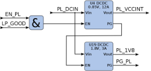
Figure 4: Programmable Logic Domain
Also as second activated Power Domain is the Full-Power Domain. Therefore, the power rail 'DCDCIN' have to be powered up and the Enable-signals 'EN_FPD' (pin J2-102) and 'EN_DDR' (J2-112) have to be asserted (max. voltage 'DCDCIN'). The resulting Power-Good-Signals 'PG_FPD' (pin J2-110) and 'PG_DDR' (J2-114) will go high after the voltages of the Full-Power Domain are properly powered up. In the following, the PSGT voltages (see figure 3) can be powered up by asserting the Enable-signal 'EN_PSGT' (pin J2-84, max. voltage 'DCDCIN'). The resulting Power-Good-Signal 'PG_PSGT' (pin J2-82) needs an extern pull-up (max. 6V).
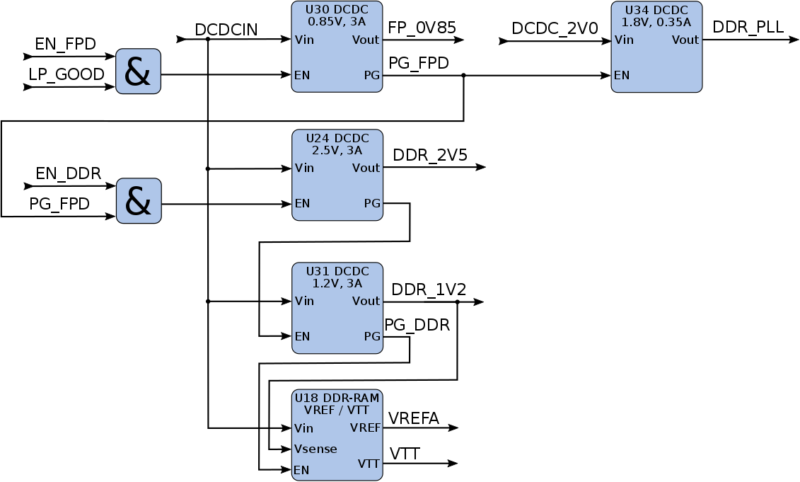
Figure 5: Full-Power Domain
The supply voltages for the MGT units of the MPSoC will be powered up last. Therefore, the power rail 'GT_DCDC' have to be powered up and the Enable-signals 'EN_GT_R' (pin J2-95), 'EN_GT_L' (pin J2-79) and 'EN_PLL_PWR' (J2-77, 7V max.) have to be asserted (max. voltage 'GT_DCDC'). The resulting Power-Good-Signals 'PG_GT_R' (pin J2-91), 'PG_GT_L' (pin J2-97) and 'PG_PLL_1V8' (J2-80) will go high after the supply voltages of the MGT units are properly powered up. The three Power-Good-Signals need an extern pull-up (max. 6V).
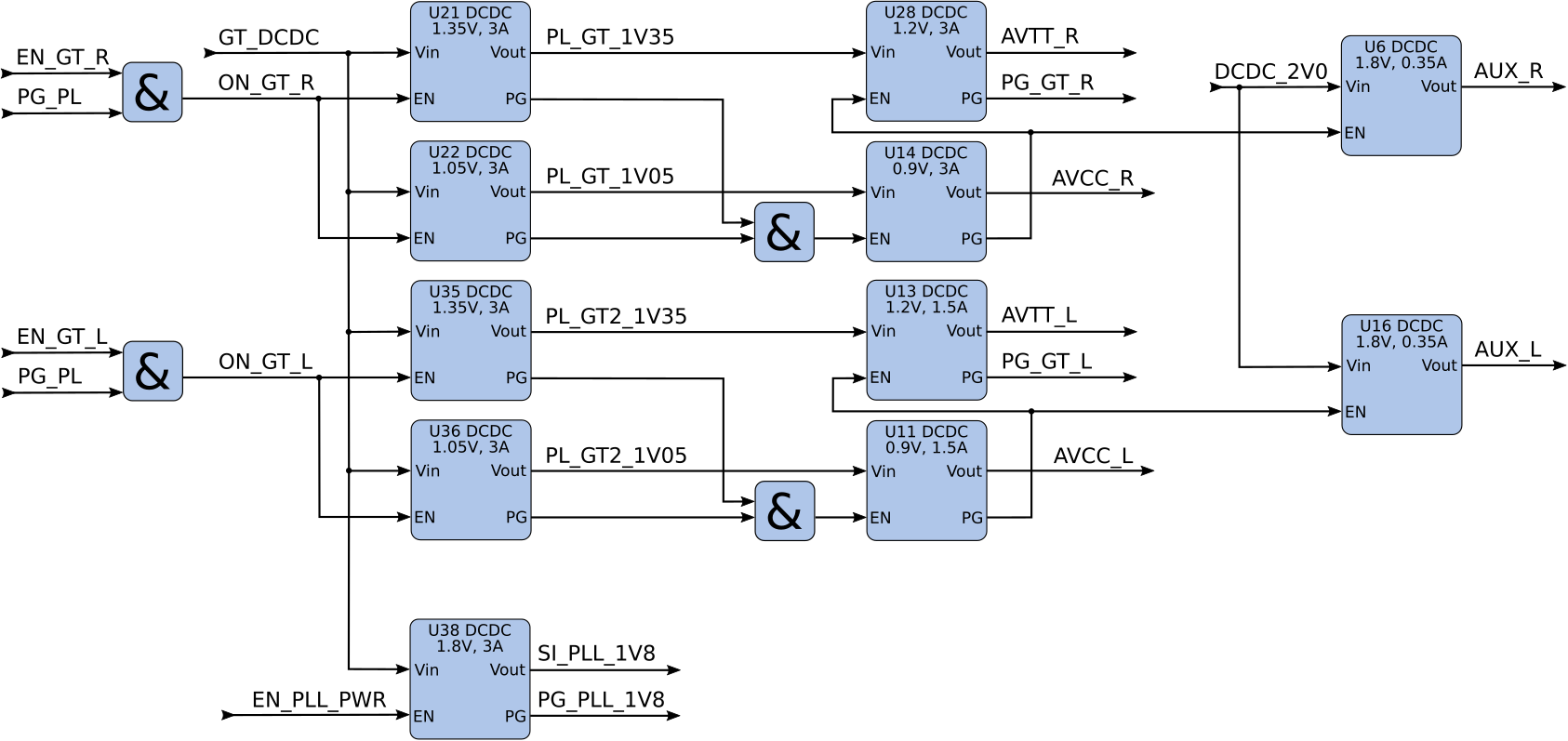
Figure 6: Powering up MGT supply voltages
The voltages 'LP_DCDC' and 'LP_0V85' are monitored by a the voltage monitor circuit U41, which generates the POR_B signal at Power-On. A manual reset is also possible the driving the MR-pin (J2-83) to GND. Leave this pin unconnected or connect to VDD (LP_DCDC) when unused.
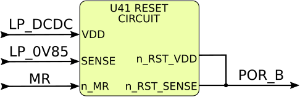
Figure 7: Voltage monitor circuit
on-board voltages of the TE0808 SoM will be powered-up in order of a determined sequence by activating the above-mentioned power rails and the Enable-Signals of the DCDC converters. The on-board voltages will be powered up at three steps.
- Low-Power Domain (LPD) and on-board Si5345A programmable clock generator supply voltage
- Programmable Logic (PL) and Full-Power Domain (FPD)
- GTH, PS GTR transceiver and DDR memory
Hence, those three power instances will be powered up consecutively and the Power-Good-Signals of the previous instance has to be asserted.
Following diagram clarifies the sequence of enabling the three power instances utilizing the DCDC converter control signals ('Enable', 'Power-Good'), which will power-up in descending order as listed in the blocks of the diagram.
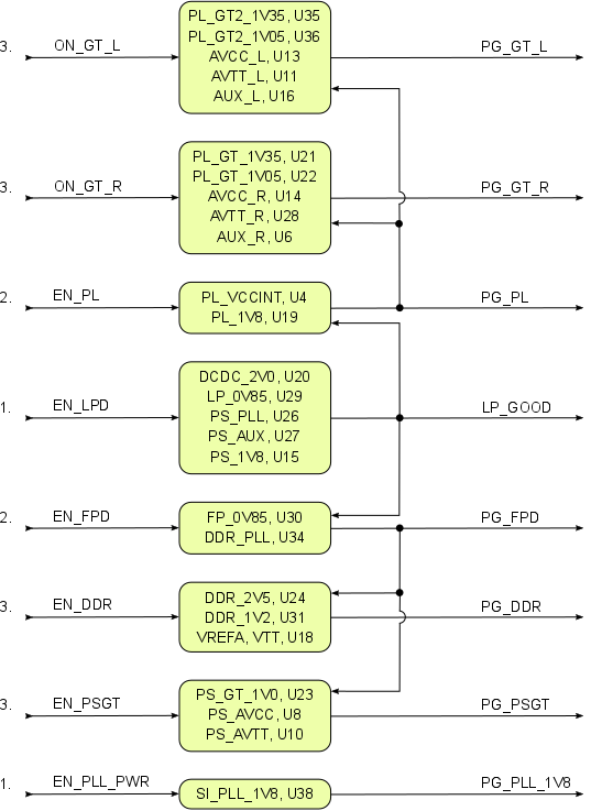
Figure 4: Power-On Sequence Utilizing DCDC Converter Control Signals
Operation Conditions of the DCDC Converter Control Signals
The control signals have to be asserted on the B2B connector J2, whereby some of the Power-Good-Signals need extern pull-up resistors.
| Enable-Signal | B2B Connector Pin | Max. Voltage | Note | Power-Good-Signal | B2B Connector Pin | Pull-up Resistor | Note | |
|---|---|---|---|---|---|---|---|---|
| EN_LPD | J2-108 | 6V | TPS82085SIL data sheet | LP_GOOD | J2-106 | 4K7, pulled up to LP_DCDC | - | |
| EN_FPD | J2-102 | DCDCIN | NC7S08P5X data sheet | PG_FPD | J2-110 | 4K7, pulled up to DCDCIN | - | |
| EN_PL | J2-101 | PL_DCIN | left floating for logic high (drive to GND for logic low) | PG_PL | J2-104 | extern pull-up needed (max. voltage 'GT_DCDC'), max. sink current 1 mA | TPS82085SIL / | |
| EN_DDR | J2-112 | DCDCIN | NC7S08P5X data sheet | PG_DDR | J2-114 | 4K7, pulled up to DCDCIN | - | |
| EN_PSGT | J2-84 | DCDCIN | NC7S08P5X data sheet | PG_PSGT | J2-82 | extern pull-up needed (max. 5.5V), max. sink current 1 mA | TPS74801 data sheet | |
| EN_GT_R | J2-95 | GT_DCDC | NC7S08P5X data sheet | PG_GT_R | J2-91 | extern pull-up needed (max. 5.5V), max. sink current 1 mA | TPS74401 data sheet | |
| EN_GT_L | J2-79 | GT_DCDC | NC7S08P5X data sheet | PG_GT_L | J2-97 | extern pull-up needed (max. 5.5V), max. sink current 1 mA | TPS74801 data sheet | |
| EN_PLL_PWR | J2-77 | 6V | TPS82085SIL data sheet | PG_PLL_1V8 | J2-80 | extern pull-up needed (max. 5.5V), max. sink current 1 mA | TPS82085SIL data sheet |
Table 14: Recommended operation conditions of DCDC converter control signals
| Warning |
|---|
| To avoid any damages |
| Warning |
| To avoid any demages to the MPSoC module, check for stabilized on-board voltages in steady state before powering up the MPSoC's I/O bank voltages VCCOx. All I/O's should be tri-stated during power-on sequence. |
Core voltages and main supply voltages have to reach stable state and their "Power Good"-signals have to be asserted before other voltages like bank's I/O voltages (VCCOx) can be powered up.
It is important that all PS and PL I/Os are 3tri-stated at power-on until the "Power Good"-signals are high, meaning that all on-module voltages have become stable and module is properly powered up.
See Xilinx datasheet DS925 for additional information. User should also check related base board documentation when intending base board design for TE0808 -03 SoM.SoM.
Voltage Monitor Circuit
The voltages 'LP_DCDC' and 'LP_0V85' are monitored by a the voltage monitor circuit U41, which generates the POR_B reset signal at Power-On. A manual reset is also possible by driving the MR-pin (J2-83) to GND. Leave this pin unconnected or connect to VDD (LP_DCDC) when unused.
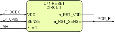
Figure 5: Voltage monitor circuit
Power Rails
Voltages on B2B | B2B J1 Pin | B2B J2 Pin | B2B J3 Pin | B2B J4 Pin | Input/ | Note |
|---|---|---|---|---|---|---|
| PL_DCIN | J1-151, J1-153, J1-157, J1-159 | - | - | - | Input | - |
| DCDCIN | - | J2-154, J2-156, J2-158, J2-160, | - | - | Input | - |
| LP_DCDC | - | J2-138, J2-140, J2-142, J2-144 | - | - | Input | - |
| PS_BATT | - | J2-125 | - | - | Input | - |
| GT_DCDC | - | - | J3-157, J3-158, J3-159, J3-160 | - | Input | - |
| PLL_3V3 | - | - | J3-152 | - | Input | U5 (programmable PLL) 3.3V nominal input |
| SI_PLL_1V8 | - | - | J3-151 | - | Output | Internal voltage level 1.8V nominal output |
| PS_1V8 | - | J2-99 | J3-148 | - | Output | Internal voltage level |
| PL_1V8 | J1-91, J1-121 | - | - | - | Output | Internal voltage level |
| DDR_1V2 | - | J2-135 | - | - | Output | Internal voltage level |
Table 15: Power rails of the MPSoC module on accessible connectors
Bank Voltages
| Bank | Type | Schematic Name / B2B connector pinsPins | Voltage | Reference Input Voltage | Voltage Range |
|---|---|---|---|---|---|
| 47 | HD | VCCO47, pins J3-43, J3-44 | user | - | max. 3.3V |
| 48 | HD | VCCO48, pins J3-15, J3-16 | user | - | max. 3.3V |
| 64 | HP | VCCO64, J4-58, J4-106 | user | VREF_64, pin J4-88 | max. 1.8V |
| 65 | HP | VCCO65, J4-69, J4-105 | user | VREF_65, pin J4-15 | max. 1.8V |
| 66 | HP | VCCO66, J1-90, J1-120 | user | VREF_66, pin J1-108 | max. 1.8V |
| 500 | PSMIOMIO | PS_1V8 | 1.8V | - | - |
| 501 | PSMIOMIO | PS_1V8 | 1.8V | - | - |
| 502 | PSMIOMIO | PS_1V8 | 1.8V | - | - |
| 503 | PSCONFIGCONFIG | PS_1V8 | 1.8V | - | - |
Table 16: Range of MPSoC module's bank voltages
B2B connectors
| 1.8V | - | - |
Table 16: Range of MPSoC module's bank voltages
B2B connectors
| Include Page | ||||
|---|---|---|---|---|
|
Variants Currently In Production
| Module Variant | Zynq Ultrascale+ MPSoC | DDR4 | Zynq Ultrascale+ MPSoC Junction Temperature | Operating Temperature Range |
|---|---|---|---|---|
| TE0808-04-09EG-1EA | XCZU9EG-1FFVC900E | 2GB | 0°C - 100°C | Extended Temperature Range |
| TE0808-04-09EG-2IB | XCZU9EG-2FFVC900I | 4GB | -40°C - 100°C | Industrial Temperature Range |
Table 17: Differences between variants of Module TE0808-04Include Page
Technical Specifications
Absolute Maximum Ratings
Parameter | Min | Max | Unit | Notes / Reference Document | |||
|---|---|---|---|---|---|---|---|
| PL_DCIN | -0.3 | 7 | V | TPS82085SIL / EN63A0QI data sheet | |||
| DCDCIN | -0.3 | 7 | V | TPS82085SIL / TPS51206PSQ TPS51206 data sheet | |||
| LP_DCDC | -0.3 | 4 | V | TPS3106K33DBVR data sheet | |||
| GT_DCDC | -0.3 | 7 | V | TPS82085SIL data sheet | |||
| PS_BATT | -0.5 | 2 | V | Xilinx DS925 data sheet | |||
| PLL_3V3 | -0.5 | 3.8 | V | Si5345/44/42 data sheet | |||
| VCCO for HD I/O banks | -0.5 | 3.4 | V | Xilinx DS925 data sheet | |||
| VCCO for HP I/O banks | -0.5 | 2 | V | Xilinx DS925 data sheet | |||
| VREF | -0.5 | 2 | V | Xilinx DS925 data sheet | |||
| I/O input voltage for HD I/O banks | -0.55 | VCCO + 0.55 | V | Xilinx DS925 data sheet | |||
| I/O input voltage for HP I/O banks | -0.55 | VCCO + 0.55 | V | Xilinx DS925 data sheet | |||
| PS I/O input voltage (MIO pins) | -0.5 | VCCO_PSIO + 0.55 | V | Xilinx DS925 data sheet, VCCO_PSIO 1.8V nominally | |||
Receiver (RXP/RXN) and transmitter | -0.5 | 1.2 | V | Xilinx DS925 data sheet | |||
Voltage on input pins of | -0.5 | VCC + 0.5 | V | NC7S08P5X data sheet, see schematic for VCC | |||
Voltage on input pins (nMR) of | -0.3 | VDD + 0.3 | V | TPS3106 data sheet, | |||
| "Enable"-signals on TPS82085SIL ('EN_PLL_PWR', 'EN_LPD') | -0.3 | 7 | V | TPS82085SIL data sheet | |||
Storage temperature (ambient) | –40 | 125 | °C | TPS82085SIL data sheet-40 | 100 | °C | ROHM Semiconductor SML-P11 Series data sheet |
| Note |
|---|
| Assembly variants for higher storage temperature range are available on request. |
Recommended Operating Conditions
| Parameter | Min | Max | Unit | Notes / Reference Document |
|---|---|---|---|---|
| PL_DCIN | 12.85 | 6 | V | EN63A0QI / TPS82085SIL data sheet |
| DCDCIN | 3.1 | 6 | V | TPS82085SIL / TPS51206PSQ data sheet |
| LP_DCDC | 2.05 | 3.6 | V | TPS3106K33DBVR TPS82085SIL / TPS3106 data sheet |
| GT_DCDC | 12.85 | 6 | V | TPS82085SIL data sheet |
| PS_BATT | 1.2 | 1.5 | V | Xilinx DS925 data sheet |
| PLL_3V3 | 3.14 | 3.47 | V | Si5345/44/42 data sheet 3.3V typical |
| VCCO for HD I/O banks | 1.14 | 3.4 | V | Xilinx DS925 data sheet |
| VCCO for HP I/O banks | 0.95 | 1.9 | V | Xilinx DS925 data sheet |
| I/O input voltage for HD I/O banks. | -0.2 | VCCO + 0.2 | V | Xilinx DS925 data sheet |
| I/O input voltage for HP I/O banks | -0.2 | VCCO + 0.2 | V | Xilinx DS925 data sheet |
| PS I/O input voltage (MIO pins) | -0.2 | VCCO_PSIO + 0.2 | V | Xilinx DS925 data sheet, VCCO_PSIO 1.8V nominally |
| Voltage on input pins of NC7S08P5X 2-Input AND Gate | 0 | VCC | V | NC7S08P5X data sheet, |
Voltage on input pins (pin 'MR) ' of | 0 | VDD | V | TPS3106 data sheet, |
| Note |
|---|
| Please check Xilinx datasheet DS925 for complete list of absolute maximum and recommended operating ratings. |
Operating Temperature Ranges
Commercial grade: 0°C to +70°C.
Industrial grade: -40°C to +85°C.
Extended grade: 0°C to +85°C.
The module operating temperature range depends also on customer design and cooling solution. Please contact us for options.
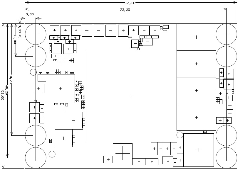
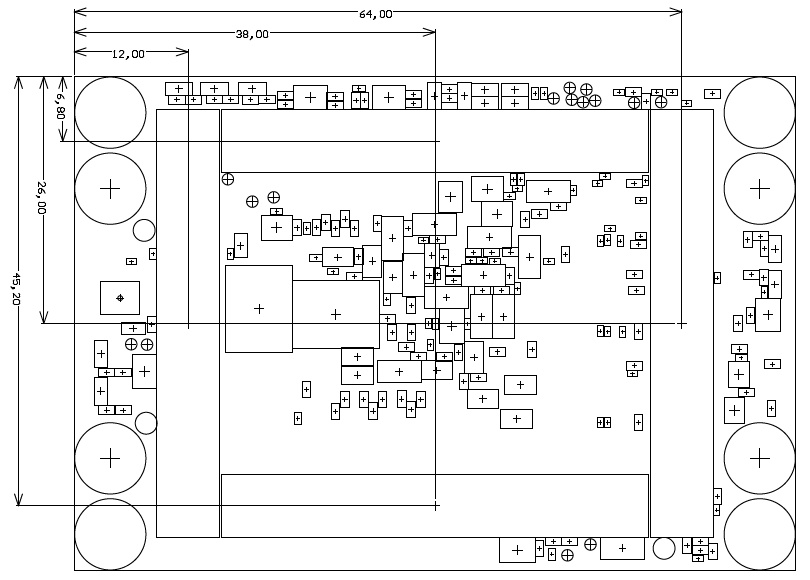
Physical Dimensions
Module size: 52 mm × 76 mm. Please download the assembly diagram for exact numbers
Mating height with standard connectors: 4mm
PCB thickness: 1.6mm
Highest part on PCB: approx. 3mm. Please download the step model for exact numbers
All dimensions are given in millimeters.
Operating Temperature Ranges
Commercial grade: 0°C to +70°C.
Industrial grade: -40°C to +85°C.
-40 ... 125 TPS82085SIL data sheet
The module operating temperature range depends also on customer design and cooling solution. Please contact us for options.
Weight
17 g - Plain module
Highest part on PCB: approx. 3mm. Please download the step model for exact numbers
All dimensions are given in millimeters.
Revision History
Hardware Revision History
| Date | Revision | Notes | Link to PCN | Documentation Link |
|---|---|---|---|---|
| - | 04 | current available module | - | - |
| - | 03 | Second production release | - | TE0808-03 |
| 2016-03-09 | 02 | First production release | - | TE0808-02 |
| - | 01 | Prototypes | - | - |
Hardware revision number is written on the PCB board together with the module model number separated by the dash.

Document Change History
| Date | Revision | Contributors | Description | ||||||||
|---|---|---|---|---|---|---|---|---|---|---|---|
| John Hartfiel, Ali Naseri | PCB REV04 Initial release | |||||||||
| 2017-02-06 | V1 | Jan Kumann | Initial document. |
Disclaimer
| Include Page | ||||
|---|---|---|---|---|
|
Overview
Content Tools