Page History
| HTML |
|---|
<!--
Template Revision 1.4 beta
--> |
| Scroll Ignore |
|---|
Download PDF version of this document. |
...
Additional assembly options are available for cost or performance optimization upon request.
| Page break |
|---|
Block Diagram
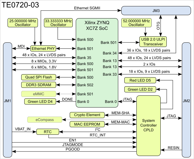
Figure 1: TE0720-03 block diagram.
Components and connections marked with dashed lines are optional or may be missing on some module variants, please contact us for additional information.
Main Components
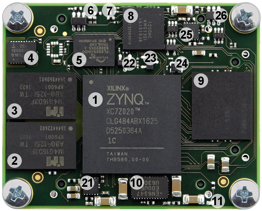
Figure 2: Main components of the module, description below.
- Xilinx Zynq XC7Z SoC, U5
- 4 Gbit DDR3/L SDRAM, U13
- 4 Gbit DDR3/L SDRAM, U12
- Low-power RTC with battery backed SRAM, U20
- 32 MByte Quad SPI Flash memory, U7
- Red LED (LED1), D5
- Green LED (LED2), D2
- System Controller CPLD, U19
- eMMC NAND Flash, U15
- 4A high-efficiency PowerSoC DC-DC step-down Converter (1V), U1
- Green LED (DONE), D4
- B2B connector Samtec Razor Beam™ LSHM-130, JM3
- B2B connector Samtec Razor Beam™ LSHM-150, JM1
- B2B connector Samtec Razor Beam™ LSHM-150, JM2
- Hi-speed USB 2.0 ULPI transceiver, U18
- Gigabit Ethernet (GbE) transceiver, U8
- Low-power programmable oscillator @ 52.000000 MHz (OTG-RCLK), U14
- Low-power programmable oscillator @ 33.333333 MHz (PS-CLK), U6
- Low-dropout regulator (VBATT), U24
- DDR termination regulator, U4
- 1.5A PowerSoC DC-DC step-down converter with integrated inductor (1.5V), U2
- Atmel CryptoAuthentication chip, U10
- 2Kbit UNI/O® serial EEPROM with EUI-48™ node identity, U17
- Low-power programmable oscillator @ 25.000000 MHz (ETH-CLK), U9
- 1.5A PowerSoC DC-DC step-down converter with integrated inductor (1.8V), U3
- 3A PFET load switch with configurable slew rate (3.3V), Q1
...
Storage device name | IC | Content | Notes |
|---|---|---|---|
Quad SPI Flash | U7 | Empty | - |
| eMMC NAND Flash | U15 | Empty | - |
| 11AA02E48T EEPROM | U17 | Pre-programmed globally unique, 48-bit node address (MAC) | - |
| System Controller CPLD | U19 | Standard firmware. | Download firmware |
Table 1: Initial state of programmable devices on module on delivery.
Signals, Interfaces and Pins
...
| Bank | Type | Voltage | B2B | I/O Count | Notes |
|---|---|---|---|---|---|
| 13 | HR GPIO | VCCIO13 | JM2 | 48 | 24 LVDS pairs |
| 13 | HR GPIO | VCCIO13 | JM2 | 2 | B13_IO0 and B13_IO25 |
| 33 | HR GPIO | VCCIO33 | JM2 | 18 | 9 LVDS pairs |
| 34 | HR GPIO | VCCIO34 | JM3 | 36 | 18 LVDS pairs |
| 35 | HR GPIO | VCCIO35 | JM1 | 48 | 24 LVDS pairs |
Table 2: General PL I/O to B2B connectors information.
PS MIO bank 500 and 501 signal connections to B2B JM1 connector, 14 PS MIOs total.
...
Overview
Content Tools