Page History
...
| PHY Signal | B2B Pin | PHY Signal | B2B Pin | |
|---|---|---|---|---|
| SOUT_N | JM3-1 | PHY_MDI1_P | JM1-10 | |
| SOUT_P | JM3-3 | PHY_MDI1_N | JM1-12 | |
| SIN_N | JM3-2 | PHY_MDI2_P | JM1-16 | |
| SIN_P | JM3-4 | PHY_MDI2_N | JM1-18 | |
| PHY_MDI0_P | JM1-4 | PHY_MDI3_P | JM1-22 | |
| PHY_MDI0_N | JM1-6 | PHY_MDI3_N | JM1-24 |
Table 8: Ethernet PHY to B2B connections.
Ethernet PHY to Zynq SoC PS MIO ETH0 connections
| PHY Signal | SoC MIO | PHY Signal | SoC MIO | |
|---|---|---|---|---|
| ETH-TXCK | 16 | ETH-RXCK | 22 | |
| ETH-TXD0 | 17 | ETH-RXD0 | 23 | |
| ETH-TXD1 | 18 | ETH-RXD1 | 24 | |
| ETH-TXD2 | 19 | ETH-RXD2 | 25 | |
| ETH-TXD3 | 20 | ETH-RXD3 | 26 | |
| ETH-TXCTL | 21 | ETH-RXCTL | 27 | |
| ETH-MDC | 52 | ETH-MDIO | 53 |
Table 9: Ethernet PHY to Zynq SoC connections.
| Page break |
|---|
USB Interface
Hi-speed USB ULPI PHY is provided by USB3320 from Microchip (U18). The ULPI interface is connected to the Zynq SoC PS USB0 via MIO28..39, bank 501.
| USB PHY Signal | Wired to | SoC MIO |
|---|---|---|
| OTG-DATA4 | U18-7 | 28 |
| OTG-DIR | U18-31 | 29 |
| OTG-STP | U18-29 | 30 |
| OTG-NXT | U18-2 | 31 |
| OTG-DATA0 | U18-3 | 32 |
| OTG-DATA1 | U18-4 | 33 |
| OTG-DATA2 | U18-5 | 34 |
| OTG-DATA3 | U18-6 | 35 |
| OTG-CLK | U18-1 | 36 |
| OTG-DATA5 | U18-9 | 37 |
| OTG-DATA6 | U18-10 | 38 |
| OTG-DATA7 | U18-13 | 39 |
Table 10: USB ULPI PHY to Zynq SoC connections.
USB PHY connection
| USB PHY Pin | SC CPLD Pin | B2B Name | Notes |
|---|---|---|---|
| REFSEL0..2 | - | - | Reference clock frequency select, all set to GND = 52.000000 MHz. |
| RESETB | B14, bank 1 | - | Active low reset. |
| CLKOUT | - | - | ULPI output clock connected to Zynq PS MIO36. |
| DP, DM | OTG-D_P, OTG-D_N | USB data lines. | |
| CPEN | VBUS_V_EN | External USB power switch active high enable signal. | |
| VBUS | - | USB-VBUS | Connect to USB VBUS via a series of resistors, see reference schematic. |
| ID | - | OTG-ID | For A-device connect to the ground, for B-device leave floating. |
| SPK_L | M5, bank 2 | - | In USB audio mode a switch connects the DM pin to the SPK_L. |
| SPK_R | M8, bank 2 | - | In USB audio mode a switch connects the DP pin to the SPK_R. |
Table 11: USB ULPI PHY connections.
I2C Interface
On-board I2C devices are connected to the System Controller CPLD which acts as a I2C bus repeater for the Zynq SoC. System Controller CPLD signals X1, X3 and X7 are routed to Zynq SoC bank 34. Exact functionality depends on the System Controller CPLD firmware.
...
Power Distribution Diagram
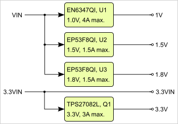
Figure 3: Power distribution diagram
| Note |
|---|
Current rating of Samtec Razor Beam™ LSHM B2B connectors is 2.0A per pin (2 adjacent pins powered). |
...
|
|
| If NOSEQ input signal from the carrier board is low (logical 0), signals ON_1V0 and ON_1V8 can be driven by System Controller CPLD to control outputs of the U1 and U3 DC-DC converters. | If NOSEQ input signal from the carrier board is high (logical 1), state of the ON_1V0 and ON_1V8 signals is irrelevant and DC-DC converters U1 and U3 outputs are always enabled. |
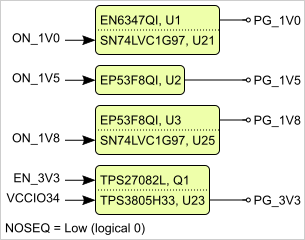
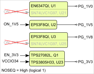
Figure 4: Power sequencing
| Note |
|---|
Initial state of the ON_1V0 and ON_1V8 signals and therefore also functionality of the NOSEQ signal depend on the System Controller CPLD firmware. |
...
All dimensions are given in millimeters.
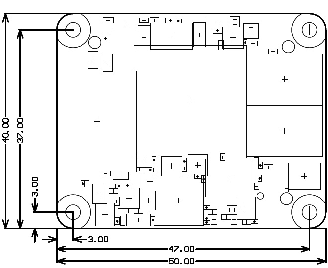
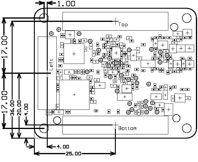
Figure 5: TE0720 modules physical dimensions
Weight
ca 23 g - Plain module
...
Date | Revision | Contributors | Description |
|---|---|---|---|
| 2017-0607-2131 | Jan Kumann | Initial document. |
...
| Include Page | ||||
|---|---|---|---|---|
|
...
Overview
Content Tools