Page History
...
The I/O signals are routed from the FPGA banks as LVDS-pairs to the connector.
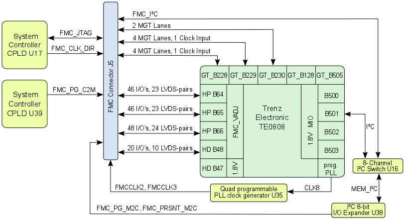
Figure 2: FMC HPC Connector
| FPGA Bank | I/O Signal Count | LVDS-pairs count | VCCO bank Voltage | Reference Clock Input from FMC Connector | Notes |
|---|---|---|---|---|---|
| Bank 48 | 20 | 10 | FMC_VADJ | 1 reference clock signal from FMC connector | - |
| Bank 64 | 46 | 23 | FMC_VADJ | 1 reference clock signal from FMC connector | bank's VREF-pin connected to FMC connector pin J5-H1 (VREF_A_M2C) |
| Bank 65 | 46 | 23 | FMC_VADJ | - | bank's VREF-pin connected to FMC connector pin J5-H1 (VREF_A_M2C) |
| Bank 66 | 48 | 24 | FMC_VADJ | - | bank's VREF-pin connected to FMC connector pin J5-H1 (VREF_A_M2C) |
...
| GT Bank | Type | Count of MGT Lanes | Schematic Names / Connector Pins | MGT Bank's Reference Clock Inputs from FMC Connector |
|---|---|---|---|---|
| 228 | GTH | 4 GTH lanes | B228_RX3_P, B228_RX3_N, pins J5-A10, J5-A11 B228_RX2_P, B228_RX2_N, pins J5-A6, J5-A7 B228_RX1_P, B228_RX1_N, pins J5-A2, J5-A3 B228_RX0_P, B228_RX0_N, pins J5-C6, J5-C7 | 1 reference clock signal (B228_CLK0) from FMC connector |
| 229 | GTH | 4 GTH lanes | B229_RX3_P, B229_RX3_N, pins J5-B12, J5-B13 B229_RX2_P, B229_RX2_N, pins J5-B16, J5-B17 B229_RX1_P, B229_RX1_N, pins J5-A18, J5-A19 B229_RX0_P, B229_RX0_N, pins J5-A14, J5-A15 | 1 reference clock signal (B229_CLK0) from FMC connector |
| 230 | GTH | 2 GTH lanes | B230_RX1_P, B230_RX1_N, pins J5-B4, J5-B5 B230_RX0_P, B230_RX0_N, pins J5-B8, J5-B9 | - |
...
The FMC connector provides pins for reference clock output to the Mezzanine module and clock input to PL banks of the MPSoC:
| Clock Signal Schematic Name | FMC Connector Pins | Direction | Clock Source | Notes |
|---|---|---|---|---|
| B228_CLK0 | J5-D4 / J5-D5 | in | FMC Connector J5 | clock signal to MGT bank 228 |
| B229_CLK0 | J5-B20 / J5-B21 | in | FMC Connector J5 | clock signal to MGT bank 229 |
| FMCCLK2 | J5-K4 / J5-K5 | out | Carrier Board PLL SI5338A U35, CLK2 | - |
| FMCCLK3 | J5-J2 / J5-J3 | out | Carrier Board PLL SI5338A U35, CLK3 | - |
| B64_L14_P / B64_L14_N | J5-H4 / J5-H5 | in | FMC Connector J5 | bank 64 clock capable pin-pair |
| B48_L6_P / B48_L6_N | J5-G2 / J5-G3 | in | FMC Connector J5 | bank 48 clock capable pin-pair |
Table 3: FMC connector pin-outs for reference clock output
...
Several VCCIO voltages are available on the FMC connector to operate the I/O's in order of the intended purpose:
| VCCIO Schematic Name | Max. Current | FMC Connector J5 Pins | Notes |
|---|---|---|---|
| 12V | C35/C37 | extern 12V power supply voltage | |
| 3V3_PER | D32/D36/D38/D40/C39 | 3.3V peripheral supply voltage | |
| FMC_VADJ | H40/G39/F40/E39 | adjustable FMC VCCIO voltage, supplied by DCDC converter U8 |
Table 5: Available VCCIO voltages on FMC connector
USB3.0 Interface
The TEBF0808 Carrier Board offers up to 4 USB3.0 superspeed ports, which are also downward compatible to USB2.0 highspeed ports. The USB3.0 ports are provided by the IC U4, Cypress Semiconductor CYUSB3324 4-port USB3.0 Hub. The pin-strap configuration option of the USB3.0 Hub U4 is disabled, so the Hub will only be configurable over the configuration EEPROM U5. The I²C interface of the EEPROM is also accessible by the MPSoC through I²C switch U16.
...
Figure 3: TEBF0808 USB3.0 interface
MPSoC's PS GT Bank 505 Peripheral Interfaces
On the PS GT Bank 505 is beside the USB3.0 Lane also the interface SATA, Display-Port and PCI Express connected.
...
Figure 4: TEBF0808 USB3.0 interface
...
MGT Interfaces SFP+ and Firefly
Overview
Content Tools