Page History
...
The Trenz Electronic TEBF0808 Carrier Board carrier board is a baseboard for the Xilinx Zynq Ultrascale+ MPSoC modules TE0808 and TE0803, which exposes the module's B2B connector pins to accessible connectors and provides a whole range of on-board components to test and evaluate the Zynq Ultrascale+ SoMs and for developing purposes. The carrier board has a Mini-ITX form factor making it capable to be fitted into a PC enclosure. On the PC enclosure's rear and front panel, essential data interfaces, sockets and connectors are accessible.
Key Features
- Mini-ITX form factor, PC Enclosure enclosure compatible
- ATX power supply connector
- Optional 12V standard power plug
- Headers
- Intel 10-pin HDA Audio
- Intel 9-pin Power-/Reset-Button, Power-/HD-LED
- PC-BEEPER
- On-board Power- / Reset-Switches
- 2x Configuration 4-bit DIP-switches
- 2x Optional 4-wire PWM fan connectors
- PCIe Slot - one PCIe lane (16 lane connector)
- CAN FD Transceiver (10 Pin IDC connector and 6-pin header)
- 4x On-board configuration EEPROMs (1x Microchip 24LC128-I/ST, 3x Microchip 24AA025E48T-I/OT)
- Dual SFP+ Connector (2x1 Cage)
- One Display-Port (single lane)
- One SATA Connector
- 2x USB3.0 A Connector (Superspeed Host Port (Highspeed at USB2.0))
- 1x USB3.0 on-board header with two ports
- FMC HPC Slot (FMC_VADJ max. VCCIO)
- FMC Fan
- Gigabit Ethernet RGMII PHY with RJ45 MegJack
- All Carrier Board peripherals' I²C-interfaces muxed to MPSoC's I²C-interface on PS bank 503
- Quad programmable PLL clock generator SI5338A
- 2x SMA coaxial connectors for clock signals
- MicroSD- / MMC-Card Socket (bootable)
- 32 Gbit on-board eMMC memory (8 banks a 4 Gbit)
- Two System Controller CPLDs Lattice MachXO2 1200 HC
- One Samtec FireFly (4 GT lanes bidirectional)
- One Samtec FireFly connector for reverse loopback
- 2x JTAG/UART header ('XMOD FTDI JTAG Adapter'-compatible) for programming MPSoC and SC CPLDs
- 20 Pin ARM JTAG Connector (PS JTAG0)
- 3x PMOD connector (GPIO's and I²C interface to SC CPLDs / MPSoC module
- Carrier SC CPLD managing power-up sequence of MPSoC module
- On-board DCDC PowerSoCs
...
The I/O signals are routed from the FPGA banks as LVDS-pairs to the connector.
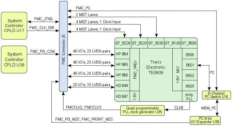
Figure 2: FMC HPC Connector
...
The MGT-banks have also clock input-pins which are exposed to the FMC connector. Following MGT-lanes are available on the FMC connectors J5:
| GT MGT Bank | Type | Count of MGT Lanes | Schematic Names / Connector Pins | MGT Bank's Reference Clock Inputs from FMC Connector |
|---|---|---|---|---|
| 228 | GTH | 4 GTH lanes | B228_RX3_P, B228_RX3_N, pins J5-A10, J5-A11 B228_RX2_P, B228_RX2_N, pins J5-A6, J5-A7 B228_RX1_P, B228_RX1_N, pins J5-A2, J5-A3 B228_RX0_P, B228_RX0_N, pins J5-C6, J5-C7 | 1 reference clock signal (B228_CLK0) from FMC connector |
| 229 | GTH | 4 GTH lanes | B229_RX3_P, B229_RX3_N, pins J5-B12, J5-B13 B229_RX2_P, B229_RX2_N, pins J5-B16, J5-B17 B229_RX1_P, B229_RX1_N, pins J5-A18, J5-A19 B229_RX0_P, B229_RX0_N, pins J5-A14, J5-A15 | 1 reference clock signal (B229_CLK0) from FMC connector |
| 230 | GTH | 2 GTH lanes | B230_RX1_P, B230_RX1_N, pins J5-B4, J5-B5 B230_RX0_P, B230_RX0_N, pins J5-B8, J5-B9 | - |
...
Table 5: Available VCCIO voltages on FMC connector
...
MIO Bank Interfaces
The TEBF0808 Carrier Board offers up to 4 USB3.0 superspeed ports, which are also downward compatible to USB2.0 highspeed ports. The USB3.0 ports are provided by the IC U4, Cypress Semiconductor CYUSB3324 4-port USB3.0 Hub. The pin-strap configuration option of the USB3.0 Hub U4 is disabled, so the Hub will only be configurable over the configuration EEPROM U5. The I²C interface of the EEPROM is also accessible by the MPSoC through I²C switch U16.
On the Upstream-side, this chip is connected to the MGT1-lane of MPSoC's PG GT bank 505 to establish the USB3.0 lane. For the USB2.0 interface, the USB3.0 HUB U4 is connected to the on-board USB2.0 PHY U9. The USB2.0 PHY U9 is connected per ULPI interface through MIO pins 52..63 to MPSoC's MIO bank 501.
Following block-diagram clarifies the wiring of the USB interface with the MPSoC.
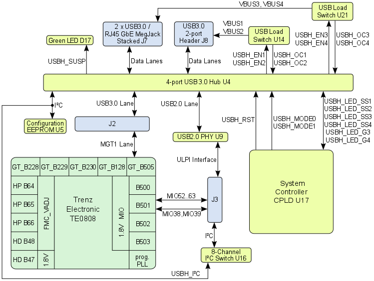
Figure 3: TEBF0808 USB3.0 interface
MPSoC's PS GT Bank 505 Peripheral Interfaces
On the PS GT Bank 505 is beside the USB3.0 Lane also the interface SATA, Display-Port and PCI Express connected.
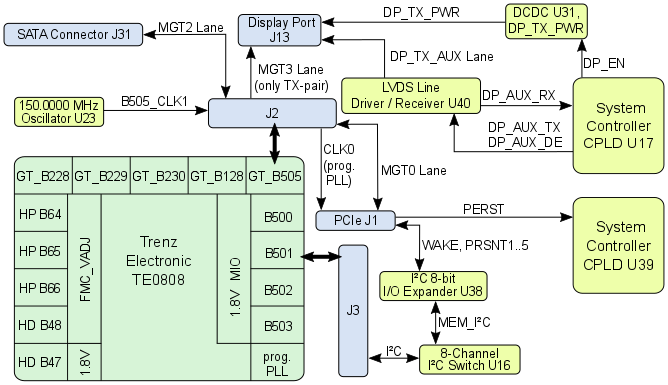
Figure 4: TEBF0808 USB3.0 interface
...
carrier board provides several interfaces, which are configured on the MIO banks 500 .. 503 of the Zynq Ultrascale+ MPSoC.
Following table contains the assignment of the MIO pins to the configured interfaces:
| MIO | Configured as | Alternate | Notes |
|---|---|---|---|
| 0..12 | Dual QSPI | - | Dual Flash Memory on TE0808 SoM; Bootable |
| 13..23 | SD0: eMMC | - | eMMC Memory U2; Bootable |
| 24, 25 | - | CPLD (U39) MUXED | - |
| 26..29 | PJTAG0 | CPLD (U17 MUXED | Bootable JTAG |
| 30 | - | CPLD (U39) MUXED | - |
| 31 | PCIe | CPLD (U39) MUXED | Same as ZCU102 |
| 32 | - | CPLD (U39) MUXED | - |
| 33 | PMU | CPLD (U39) MUXED | Same as ZCU102 |
| 34..37 | DisplayPort Aux | CPLD (U39) MUXED | - |
| 38, 39 | I2C0 | - | - |
| 40, 41 | CAN1 | CPLD (U39) MUXED | - |
| 42, 43 | UART0 | CPLD (U39) MUXED | - |
| 44 | I2C Interrupt | CPLD (U39) MUXED | - |
| 45..51 | SD1: SD | - | Bootable MikeoSD / MMC Card |
| 52..63 | USB0 | - | - |
| 64..75 | GEM3 | - | Ethernet RGMII |
| 76, 77 | MDC / MDIO | - | Ethernet RGMII |
Table 5: MIO Assignment
On the carrier board there are up to 4 USB3.0 Super Speed ports available, which are also downward compatible to USB2.0 High Speed ports. The USB3.0 ports are provided by the IC U4, Cypress Semiconductor CYUSB3324 4-port USB3.0 Hub. The pin-strap configuration option of the USB3.0 Hub U4 is disabled, so the Hub will only be configurable over the configuration EEPROM U5. The I²C interface of the EEPROM is also accessible by the MPSoC through I²C switch U16.
On the Upstream-side, this chip is connected to the MGT1 lane of MPSoC's PG GT bank 505 to establish the USB3.0 data lane. For the USB2.0 interface, the USB3.0 HUB U4 is connected to the on-board USB2.0 PHY U9. The USB2.0 PHY U9 is connected per ULPI interface (MIO pins 52..63) to MPSoC's MIO bank 501.
Further interfaces of the MIO bank:
- SDIO port with muxed MikroSD and MMC Socket
- Gigabit Ethernet connected per RGMII
- eMMC Memory
- 4 x user configuration EEPROMs with I²C interface
Following block-diagram visualizes the interfaces of the MIO bank at the Zynq Ultrascale+ MPSoC and their associated on-board peripherals.
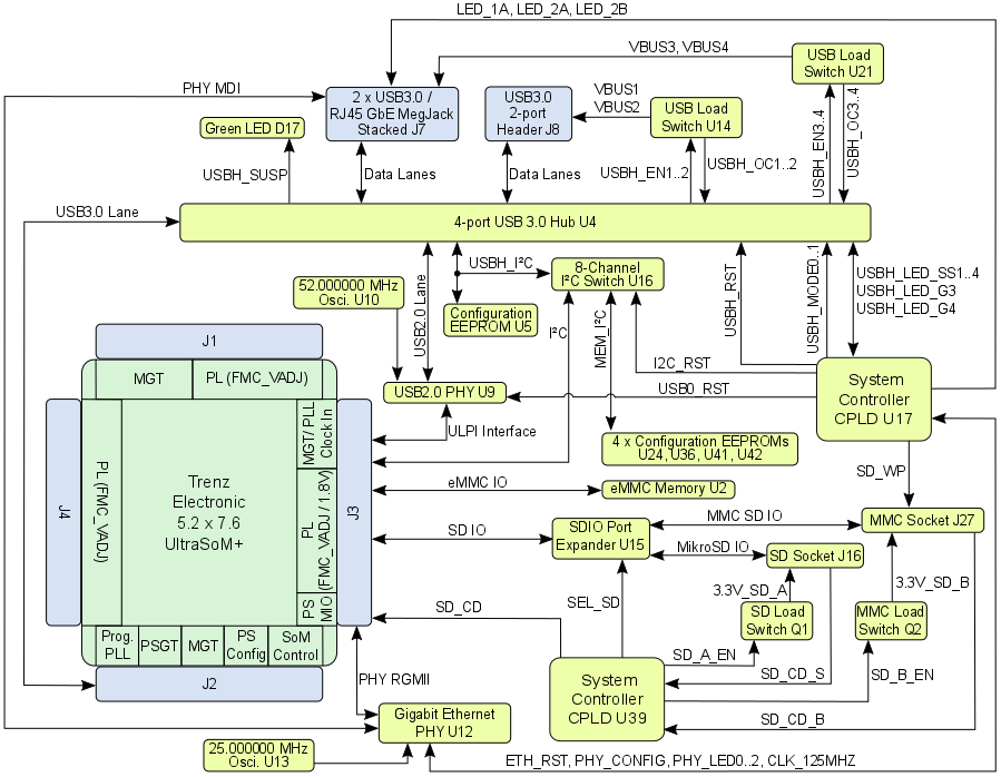
Figure 3: TEBF0808 MIO Interfaces
MPSoC's PS GT Bank 505 Interfaces
On the PS GT Bank 505 provides beside the USB3.0 Lane also following interfaces:
- SATA (PS GT bank 505, MGT2 Lane)
- Display-Port (PS GT bank 505, MGT3 Lane, only TX-pair routed)
- PCI Express (PS GT bank 505, MGT0 Lane)
| Function | MGT Lane | Ref Clock | Clock Source | Comment |
|---|---|---|---|---|
| PCIe | PS 0 | 100 MHz | Si5345 (CLK0 of prog. PLL on mounted SoM) | - |
| USB3 | PS 1 | 100 MHz | Optional Oscillator U6 | - |
| SATA | PS 2 | 150 MHz | Oscillator U23 | - |
| DP.0 | PS 3 | 27 MHz | - | Display Port |
Table 6: PS GT Lane Assignment
Following block diagram shows the wiring of the MGT Lanes of the PS GT bank 505 to the particular high speed data interfaces:
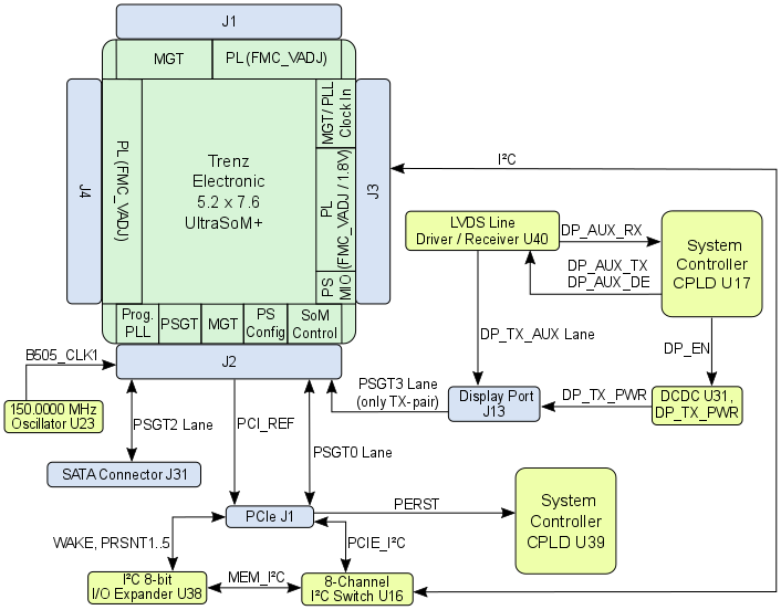
Figure 4: TEBF0808 PS GT Bank 505 Interface
MGT Interfaces SFP+ and Firefly
The TEBF0808 carrier board provides the high speed MGT interface connectors "SFP+" (Enhanced small form-factor pluggable) and Samtec "FireFly". Each of this connectors are capable of data transmission rates up to 10 Gbit/s.
| Function | MGT Lane | Ref Clock | Clock Source | Comment |
|---|---|---|---|---|
| FireFly | B128 MGT Lanes 0..3 | - | - | - |
| SFP | B230 MGT Lane 2 | 125/156.25 MHz | Si5345 (CLK7 of prog. PLL on mounted SoM) | - |
| SFP | B230 MGT Lane 3 | 125/156.25 MHz | Si5345 (CLK7 of prog. PLL on mounted SoM) | - |
Table 6: MGT Lane Assignment
Following block diagram show the wiring of the MGT lanes to the particular interface connectors:
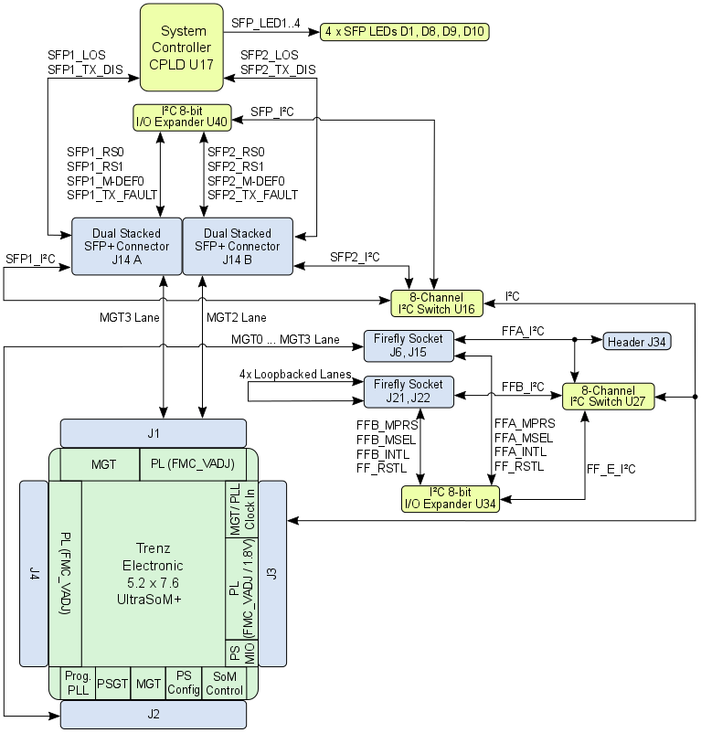
Figure 5: TEBF0808 MGT Interfaces
As shown on the block diagram, the FireFly connector pair J21, J22 provides four reversed looped back MGT lanes. To test any of the on-board MGT lanes or of an extern device, 4 RX/TX differential pairs are bridged on the connector, hence the transmitted data on these MGT lanes flows back to their sources in a loop-back circuit without intentional processing or modification.
CAN FD Interface and PMOD Connectors
On the carrier board there is a CAN FD (CAN with Flexible Data-Rate) interface available which is accessible on the CAN headers J24 (10-pin IDC connector) or J29 (6-pin header), which are connected to the CAN FD transceiver U30.
Additionally the carrier board provides PMOD connectors with GPIO and I²C interface. Following table
| PMOD | Interface | Connected with | Notes |
|---|---|---|---|
| P1 | GPIO | HP Bank 65 of MPSoC (4 I/O's) System Controller CPLD U17 (I/O's) | Voltage translation via IC U33 with direction control, only singled-ended signaling possible |
| P2 | I²C | 8-channel I²C Switch U27 | Accessible on MPSoC's I²C interface |
| P3 | I²C | 8-channel I²C Switch U27 | Accessible on MPSoC's I²C interface |
Table 7: PMOD Pin Assignment
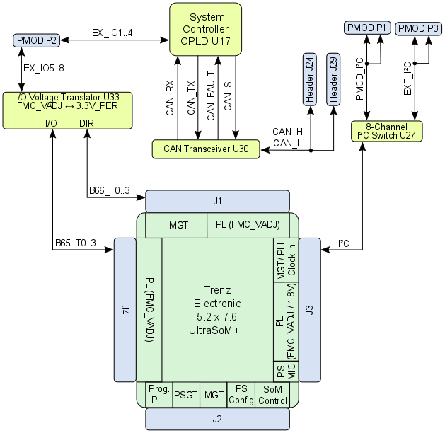
Figure 6: TEBF0808 CAN Interfaces, PMOD
Intel PC and FAN Headers
The TEBF0808 carrier board provides with its Mini-ITX form factor the possibility to encase the board in a PC Enclosure. For this purpose, the board is equipped with several Intel PC compatible headers to connect them to the PC Enclosure.
Pins are available for following PC front panel elements
- Reset Button
- Power Button
- Power LED
- Hard Disc (HD) LED
- Intel High Definition Audio (HDA) Jacks
| Header | Pins | Connected to | Function | Notes |
|---|---|---|---|---|
| J10 | Pin 1, HD LED+ | SC CPLD U39 | HD LED Anode | also connected to switch button S1 also connected to switch button S2 |
| J9 | Pin 1, PORT1L | 24-bit Audio Codec IC U3 | Microphone Jack Left Microphone Jack Right Audio Out Jack Left Audio Out Jack Right Jack Detect / Mic in | - |
| J23 | Pin 4, S1 | SC CPLD U39 | PC compatible Beeper | - |
| J26 | Pin 3, F1SENSE | SC CPLD U39 | 4-wire PWM FAN connector | - |
| J35 | Pin 3, F2SENSE | SC CPLD U39 | 4-wire PWM FAN connector | optional load switch U48 to turn off/on FAN |
| J19 | - | Load Switch Q3 (5V DCDC) | 2-wire FAN connector | Fan off/on switchable by signal 'FAN_FMC_EN' on SC CPLD U39 |
PC compatible Headers
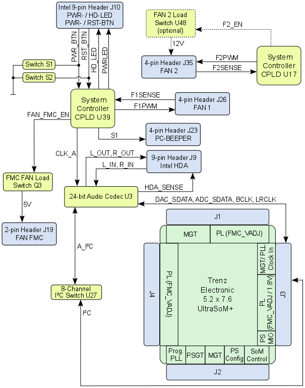
Figure 7: TEBF0808 PC Compatible Headers
JTAG Interface
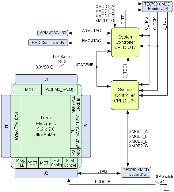
Overview
Content Tools