Page History
...
Following table describes how to set the control lines to configure the desired boot mode:
| Boot Mode | MIO5 (BOOTMODE_1) | MIO4 (BOOTMODE) | MIO3 | Note |
|---|---|---|---|---|
JTAG | 0 | 0 | 0 | - |
| NOR | 0 | 0 | 1 | MIO3 pin is shared with QSPI Flash Memory (QSPI-DQ1) |
| NAND | 0 | 1 | 0 | - |
| QSPI Flash Memory | 1 | 0 | 0 | standard mode in current configuration |
| SD-Card | 1 | 1 | 0 | SD-Card on base board necessary |
Table 11: Selectable boot modes
...
Figure 8: TEBF0808 System Controller CPLDs
Programmable PLL Clock Generator and Reference Clock Oscillators
...
Once running, the frequency and other parameters can be changed by programming the device using the I2C-bus connected through I²C switch U16 between the Zynq module (master) and reference clock signal generator (slave).
| Si5338A ( |
|---|
| U35) Input | Signal Schematic Name | Note |
|---|---|---|
IN1/IN2 | CLK8_P, CLK8_N | Reference clock signal from Si5345 (CLK8 of prog. PLL on mounted SoM) |
IN3 | reference clock signal from oscillator SiTime SiT8008BI (U7) | 25.000000 MHz fixed frequency. |
IN4/IN6 | pins put to GND | LSB (pin 'IN4') of the default I²C-adress 0x70 not activated. |
IN5 | not connected | - |
| Si5338A ( |
| U35) Output | Signal Schematic Name | Note |
|---|---|---|
CLK0 A/B | SC_CLK0 | Reference clock signal to SC CPLD U17 (single-ended signaling) |
CLK1 A/B | SC_CLK1 | Reference clock signal to SC CPLD U17 (single-ended signaling) |
CLK2 A/B | FMCCLK2_P, FMCCLK2_N | Clock signal routed to FMC connector J5, pins J5-K4 / J5-K5 |
| CLK3 A/B | FMCCLK3_P, FMCCLK3_N | Clock signal routed to FMC connector J5, pins J5-J2 / J5-J3 |
Table 9: Pin description of PLL clock generator Si5338A
...
| Note |
|---|
Si5338 OTP ROM is not programmed by default at delivery, so it is customers responsibility to either configure Si5338 during FSBL or then use SiLabs programmer and burn the OTP ROM with customer fixed clock setup. |
Si5345 Si5338 OTP can only be programmed two times, as different user configurations may required different setup, TEBF0808 is normally shipped with blank OTP.
For more information Si5338 at SiLabs.
...
The TEBF0808 carrier board is equipped several on-board oscillators to provide the Zynq Ultrascale+ MPSoC's PS and PL banks and the on-board peripherals with reference clock-signals:
| Clock Source | Schematic Name | Frequency | Clock Input Destination |
|---|---|---|---|
| SiTime SiT8008BI oscillator, U21 | - | 25.000000 MHz | Quad PLL clock generator U16, pin 3 |
SiTime SiT8008BI oscillator, U12 | PS_CLK | 33.333333 MHz | Bank 500 (MIO0 bank), pin B24 |
| SiTime SiT8008BI oscillator, U33 | OTG-RCLK | 52.000000 MHz | USB 2.0 transceiver PHY U32, pin 26 |
| SiTime SiT8008BI oscillator, U9 | ETH_CLKIN | 25.000000 MHz | Gigabit Ethernet PHY U7, pin 34 |
Table 10: Reference clock signal oscillators
...
High-speed USB ULPI PHY
USB PHY (U32) is provided by USB3320 from Microchip. The ULPI interface is connected to the Zynq PS USB0. I/O voltage is fixed at 1.8V and PHY reference clock input is supplied from the on-board 52.000000 MHz oscillator (U33).
| PHY Pin | ZYNQ Pin | B2B Name | Notes |
|---|---|---|---|
| ULPI | MIO28 ... MIO39 | - | Zynq USB0 MIO pins are connected to the PHY. |
| REFCLK | - | - | 52MHz from on board oscillator (U33). |
| REFSEL[0..2] | - | - | All pins set to GND selects the external reference clock frequency (52.000000 MHz). |
| RESETB | MIO7 | - | Low active USB PHY Reset (pulled-up to PS_1.8V). |
| CLKOUT | MIO36 | - | Set to logic high to select reference clock (oscillator U33) operation mode. |
| DP, DM | - | OTG_D_P, OTG_D_N, pin J2-149 / J2-151 | USB data lines. |
| CPEN | - | VBUS_V_EN, pin J2-141 | External USB power switch active-high enable signal. |
| VBUS | - | USB_VBUS, pin J2-145 | Connect to USB VBUS via a series of resistors, see reference schematics. |
| ID | - | OTG_ID, pin J2-143 | For an A-device connect to the ground. For a B-device, leave floating. |
Table 8: USB PHY interface connections
...
On-board Gigabit Ethernet PHY (U7) is provided with Marvell Alaska 88E1512 IC. The Ethernet PHY RGMII interface is connected to the Zynq Ethernet0 PS GEM0. I/O voltage is fixed at 1.8V for HSTL signaling. The reference clock input of the PHY is supplied from the on-board 25.000000 MHz oscillator (U9). The 125MHz PHY output clock (PHY_CLK125M) is routed to the B2B connector J2 pin 150.
| PHY Pin | ZYNQ PS | B2B | Notes |
|---|---|---|---|
| MDC/MDIO | MIO52, MIO53 | - | - |
| PHY LEDs | - | PHY_LED0: J2-144 | - |
| PHY_LED2 / INTn: | - | J2-148 | Active low interrupt line |
| PHY_CLK125M | - | J2-150 | 125 MHz Ethernet PHY clock out |
| CONFIG | - | - | Permanent logic high |
| RESETn | MIO9 | - | Active low reset line |
| RGMII | MIO16 ... MIO27 | - | Reduced Gigabit Media Independent Interface |
| SGMII | - | - | Serial Gigabit Media Independent Interface |
| MDI | - | PHY_MDI0: J2-120 / J2-122 PHY_MDI1: J2-126 / J2-128 PHY_MDI2: J2-132 / J2-134 PHY_MDI3: J2-138 / J2-140 | Media Dependent Interface |
Table 7: Ethernet PHY interface connections
...
I²C Switches
The I2C interface on B2B connector J2 pins 119 (I2C_33_SCL) and 121 (I2C_33_SDA) have PS_3.3V as reference voltage.
The I2C bus works internally on module with reference voltage 1.8V, on the Zynq chip it is connected to the PS I2C interface via PS MIO bank 500, pins MIO10 and MIO11.
| MIO | Signal Schematic Name | Notes |
|---|---|---|
| 10 | I2C_SCL | 1.8V reference voltage |
| 11 | I2C_SDA | 1.8V reference voltage |
Table 9: MIO-pin assignment of the module's I2C interface
...
I2C addresses for on-board devices are listed in the table below:
| I2C Device | I2C Address | Notes |
|---|---|---|
| Zynq chip U1, bank 500 (PS MIO), pins MIO10 (SCL), MIO11 (SDA) | User programmable | Configured as I2C by default |
| Quad programmable PLL clock generator U16: pins 12 (SCL), 19 (SDA) | 0x70 | - |
| MAC Address EEPROM U23, pins 1 (SCL), 3 (SDA) | 0x53 | - |
| SC CPLD U2, bank 2, pins 16 (SDA), 17 (SCL) | User programmable | - |
| RTC, U24 | 0x6F | - |
| RTC RAM, U24 | 0x57 | - |
Table 10: Module's I2C-interfaces overview
...
An temperature compensated Intersil ISL12020M is used as Real Time Clock (U24). Battery voltage must be supplied to the clock from the base board via pin 'VBAT_IN' (J1-146). Battery backed registers can be accessed over I2C bus at slave address 0x6F. General purpose RAM of the RTC can be accessed at I2C slave address 0x57. RTC IC is supported by Linux so it can be used as hwclock device. The interrupt line 'RTC_INT' of the RTC is connected to System Controller CPLD bank 3 pin 4.
On-board LEDs
LED | Color | Connected to | Description and Notes |
|---|---|---|---|
| D1 | red | DONE signal (PS Configuration Bank 503) | This LED goes ON when power has been applied to the module and stays ON until MPSoC's programmable logic is configured properly. |
Table 14: LED's description
Power and Power-On Sequence
Power Consumption
The maximum power consumption of a module mainly depends on the design which is running on the FPGA.
Xilinx provide a power estimator excel sheets to calculate power consumption. It's also possible to evaluate the power consumption of the developed design with Vivado. See also Trenz Electronic Wiki FAQ.
| Power Input Pin | Typical Current |
|---|---|
| DCDCIN | TBD* |
| LP_DCDC | TBD* |
| PL_DCIN | TBD* |
| PS_BATT | TBD* |
Table 15: Maximum current of power supplies. *to be determined soon with reference design setup.
...
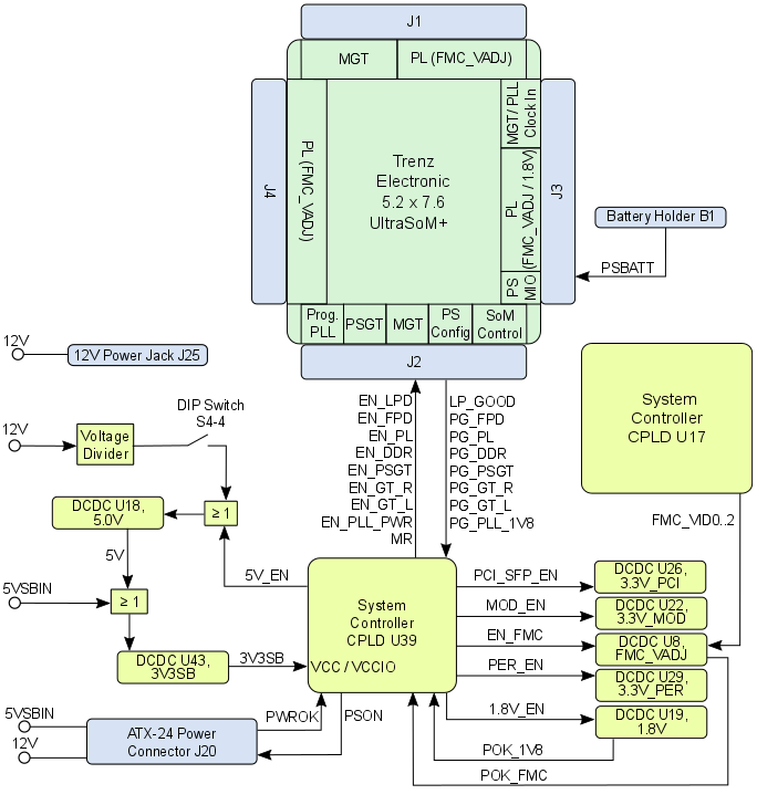
There are following dependencies how the initial voltages of the power rails on the B2B connectors are distributed to the on-board DCDC converters, which power up further DCDC converters and the particular on-board voltages:
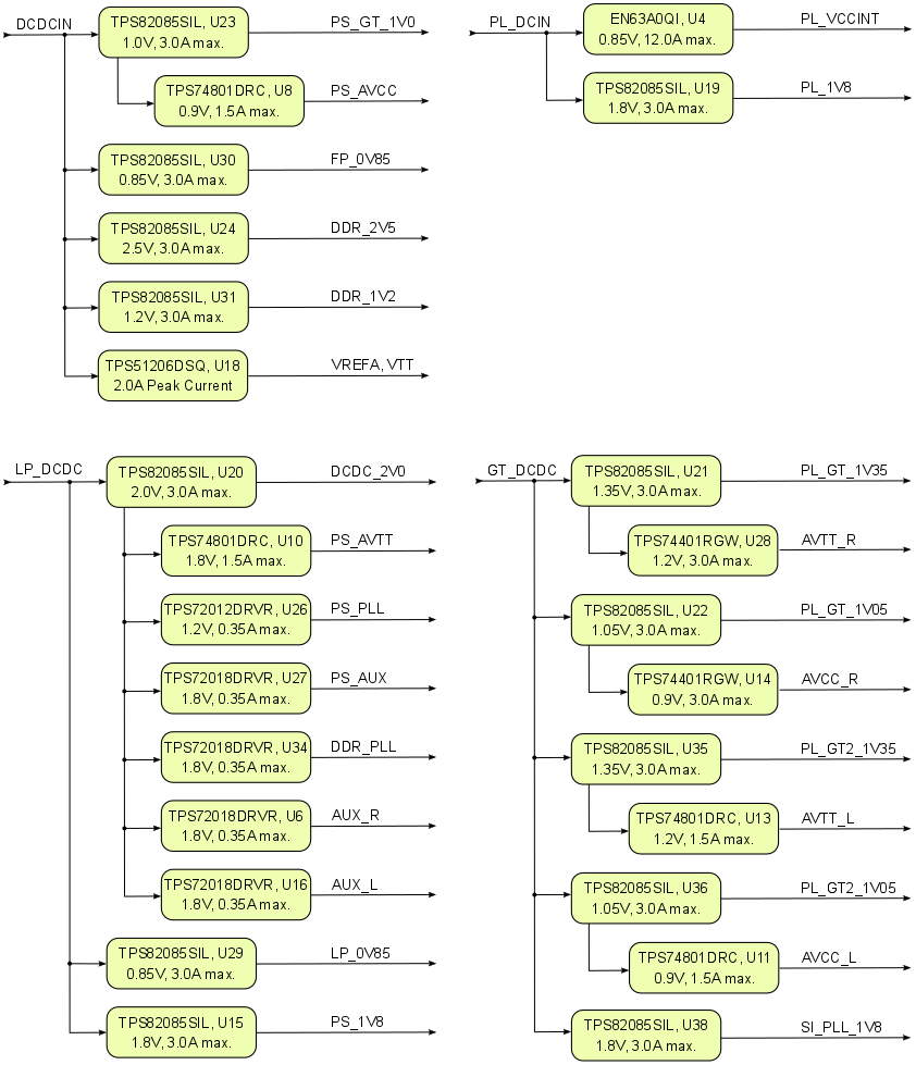
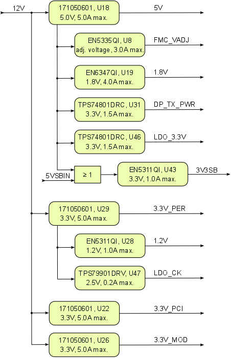
Figure 3: Power Distribution Diagram
...
Following diagram clarifies the sequence of enabling the three power instances utilizing the DCDC converter control signals ('Enable', 'Power-Good'), which will power-up in descending order as listed in the blocks of the diagram.
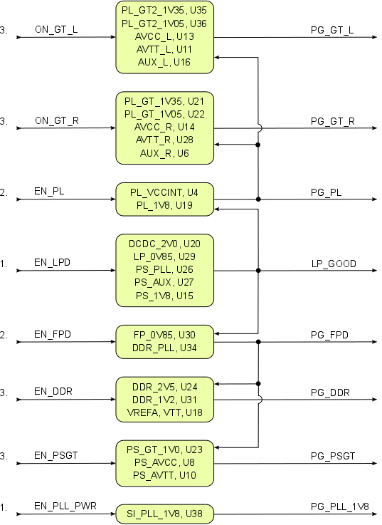
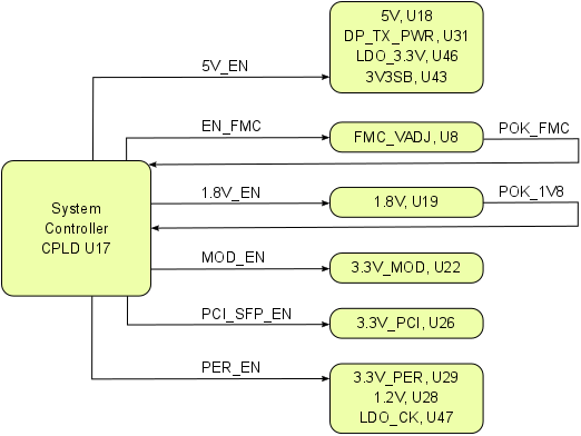
Figure 4: Power-On Sequence Utilizing DCDC Converter Control Signals
| Warning |
|---|
| To avoid any damages to the MPSoC module, check for stabilized on-board voltages in steady state before powering up the MPSoC's I/O bank voltages VCCOx. All I/O's should be tri-stated during power-on sequence. |
...
See Xilinx datasheet DS925 for additional information. User should also check related base board documentation when intending base board design for TE0808 SoM.
Power Rails
Voltages on B2B | B2B J1 Pin | B2B J2 Pin | B2B J3 Pin | B2B J4 Pin | Input/ | Note |
|---|---|---|---|---|---|---|
| PL_DCIN | J1-151, J1-153, J1-157, J1-159 | - | - | - | Input | - |
| DCDCIN | - | J2-154, J2-156, J2-158, J2-160, | - | - | Input | - |
| LP_DCDC | - | J2-138, J2-140, J2-142, J2-144 | - | - | Input | - |
| PS_BATT | - | J2-125 | - | - | Input | - |
| GT_DCDC | - | - | J3-157, J3-158, J3-159, J3-160 | - | Input | - |
| PLL_3V3 | - | - | J3-152 | - | Input | U5 (programmable PLL) 3.3V nominal input |
| SI_PLL_1V8 | - | - | J3-151 | - | Output | Internal voltage level 1.8V nominal output |
| PS_1V8 | - | J2-99 | J3-148 | - | Output | Internal voltage level |
| PL_1V8 | J1-91, J1-121 | - | - | - | Output | Internal voltage level |
| DDR_1V2 | - | J2-135 | - | - | Output | Internal voltage level |
Table 17: Power rails of the MPSoC module on accessible connectors
B2B connectors
Bank Voltages
...
Table 18: Range of MPSoC module's bank voltages
B2B connectors
...
Technical Specifications
Absolute Maximum Ratings
...
Parameter
...
Unit
...
Notes / Reference Document
...
Receiver (RXP/RXN) and transmitter
(TXP/TXN) absolute input voltage
...
Voltage on input pins of
NC7S08P5X 2-Input AND Gate
...
Voltage on input pins (nMR) of
TPS3106K33DBVR Voltage Monitor, U41
...
TPS3106 data sheet,
VDD = LP_DCDC
...
Storage temperature (ambient)
...
-40
...
°C
...
| Include Page | ||||
|---|---|---|---|---|
|
Technical Specifications
Absolute Maximum Ratings
Parameter | Min | Max | Unit | Notes / Reference Document |
|---|---|---|---|---|
| PL_DCIN | -0.3 | 7 | V | TPS82085SIL / EN63A0QI data sheet |
| DCDCIN | -0.3 | 7 | V | TPS82085SIL / TPS51206 data sheet |
| LP_DCDC | -0.3 | 4 | V | TPS3106K33DBVR data sheet |
| GT_DCDC | -0.3 | 7 | V | TPS82085SIL data sheet |
| Note |
|---|
| Assembly variants for higher storage temperature range are available on request. |
Recommended Operating Conditions
| Parameter | Min | Max | Unit | Notes / Reference Document |
|---|---|---|---|---|
| PL_DCIN | 2.5 | 6 | V | EN63A0QI / TPS82085SIL data sheet |
| DCDCIN | 3.1 | 6 | V | TPS82085SIL / TPS51206PSQ data sheet |
| LP_DCDC | 2.5 | 3.6 | V | TPS82085SIL / TPS3106 data sheet |
| Note |
|---|
| Assembly variants for higher storage temperature range are available on request. |
Recommended Operating Conditions
...
NC7S08P5X data sheet,
see schematic for VCC
...
Voltage on input pin 'MR' of
TPS3106K33DBVR Voltage Monitor, U41
...
TPS3106 data sheet,
VDD = LP_DCDC
| Note |
|---|
| Please check Xilinx datasheet DS925 for complete list of absolute maximum and recommended operating ratings. |
Operating Temperature Ranges
...
All dimensions are given in millimeters.

Revision History
Hardware Revision History
| Date | Revision | Notes | Link to PCN | Documentation Link |
|---|---|---|---|---|
| - | 04 | First production silicon | - | - |
| - | 03 | Second ES production release | - |
| TEBF0808-03 |
| - |
| 02 | First ES production release | - |
| TEBF0808-02 | ||||
| - | 01 | Prototypes | - | - |
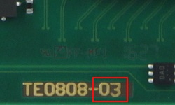
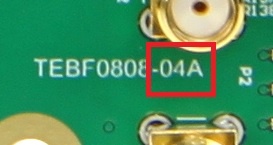
Hardware revision number is written on the PCB board together with the module model number separated by the dash.
Document Change History
| Date | Revision | Contributors | Description | |||||
|---|---|---|---|---|---|---|---|---|
|
| Ali Naseri |
- PCB REV04 Initial release
- update boot mode section
| Initial document |
Disclaimer
| Include Page | ||||
|---|---|---|---|---|
|
Overview
Content Tools