Page History
...
- Mini-ITX form factor, PC enclosure compatible
- ATX-24 power supply connector
- Optional 12V standard power plug
- Headers
- Intel 10-pin HDA Audio
- Intel 9-pin Power-/Reset-Button, Power-/HD-LED
- PC-BEEPER
- On-board Power- / Reset-Switches
- 2x Configuration 4-bit DIP-switches
- 2x Optional 4-wire PWM fan connectors
- PCIe Slot - one PCIe lane (16 lane connector)
- CAN FD Transceiver (10 Pin IDC connector and 6-pin header)
- 4x On-board configuration EEPROMs (1x Microchip 24LC128-I/ST, 3x Microchip 24AA025E48T-I/OT)
- Dual SFP+ Connector (2x1 Cage)
- One Display-Port (single lane)
- One SATA Connector
- 2x USB3.0 A Connector (Superspeed Host Port (Highspeed at USB2.0))
- 1x USB3.0 on-board header with two ports
- FMC HPC Slot (FMC_VADJ max. VCCIO)
- FMC Fan
- Gigabit Ethernet RGMII PHY with RJ45 MegJack
- All Carrier Board peripherals' I²C-interfaces muxed to MPSoC's I²C-interface on PS bank 503
- Quad programmable PLL clock generator SI5338A
- 2x SMA coaxial connectors for clock signals
- MicroSD- / MMC-Card Socket (bootable)
- 32 Gbit on-board eMMC memory (8 banks a 4 Gbit)
- Two System Controller CPLDs Lattice MachXO2 1200 HC
- One Samtec FireFly (4 GT lanes bidirectional)
- One Samtec FireFly connector for reverse loopback
- 2x JTAG/UART header ('XMOD FTDI JTAG Adapter'-compatible) for programming MPSoC and SC CPLDs
- 20 Pin ARM JTAG Connector (PS JTAG0)
- 3x PMOD connector (GPIO's and I²C interface to SC CPLDs / MPSoC module
- Carrier SC CPLD managing power-up sequence of MPSoC module
- On-board DCDC DC-DC PowerSoCs
Additional assembly options are available for cost or performance optimization upon request.
...
| VCCIO Schematic Name | FMC Connector J5 Pins | Notes |
|---|---|---|
| 12V | C35/C37 | extern 12V power supply |
| 3V3_PER | D32/D36/D38/D40/C39 | 3.3V peripheral supply voltage |
| FMC_VADJ | H40/G39/F40/E39 | adjustable FMC VCCIO voltage, supplied by DCDC DC-DC converter U8 |
Table 5: Available VCCIO voltages on FMC connector
...
| Header | Pin Name | Function | Connected to | Notes |
|---|---|---|---|---|
| J10 | Pin 1, HD LED+ | HD LED Anode | SC CPLD U39 | Reset und Power Switch-pins are also connected to switch buttons S1 and S2 |
| J9 | Pin 1, PORT1L | Microphone Jack Left Microphone Jack Right Audio Out Jack Left Audio Out Jack Right Jack Detect / Mic in Ground | 24-bit Audio Codec IC U3 | - |
| J23 | Pin 1, 3V3SB Pin 4, S1 | 3.3V DC Supply PC compatible Beeper | SC CPLD U39 | - |
| J26 | Pin 1, GND | Ground 12V DC Supply RPM PWM | SC CPLD U39 | 4-wire PWM FAN connector |
| J35 | Pin 1, GND | Ground 12V DC Supply RPM PWM | SC CPLD U39 | 4-wire PWM FAN connector |
| J19 | Pin 1, GND | Ground 5V DC Supply | Load Switch Q3 (5V DCDCDC) | 2-wire FAN connector Fan off/on switchable by signal 'FAN_FMC_EN' on SC CPLD U39 |
...
Power and Power-On Sequence
...
Power Consumption
The maximum power consumption of a module mainly depends on the design which is running on the FPGA.
Xilinx provide a power estimator excel sheets to calculate power consumption. It's also possible to evaluate the power consumption of the developed design with Vivado. See also Trenz Electronic Wiki FAQ.
Power
...
Management
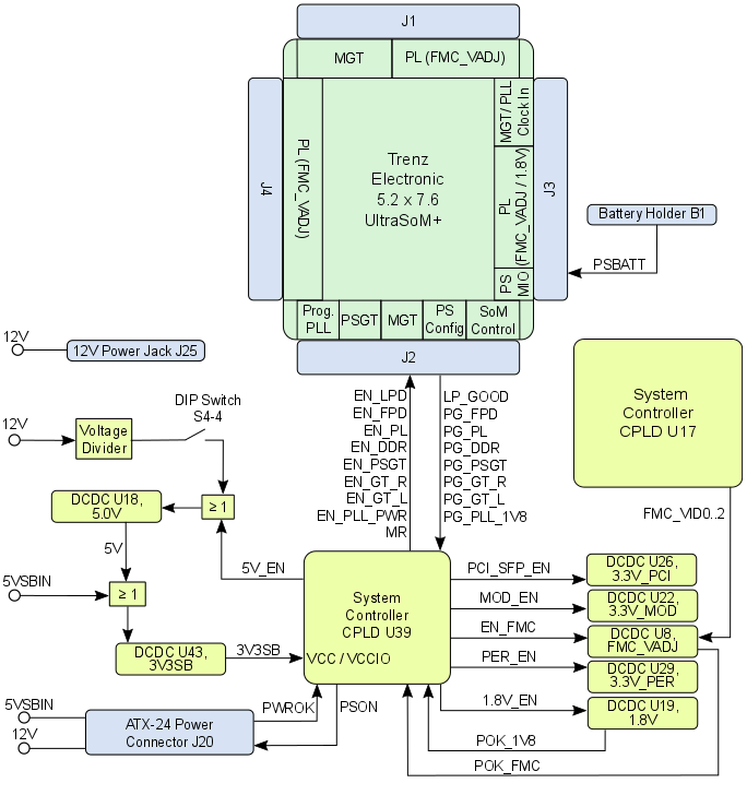
The TEBF0808 carrier board manages both the power-on sequence of the mounted TE0808 SoM and the on-board DC-DC converters via System Controller CPLD U39.
The power-on sequence of the TE0808 SoM is managed by utilizing the SoM's DC-DC converter control signals ('Enable', 'Power-Good'), so the DC-DC converters of the SoM dedicated to the particular Power Domains of the Zynq Ultrascale+ MPSoC will be powerer-up in a specific sequence to meet the recommended criteria to power up the Xilinx Zynq Ultrascale+ MPSoC properly.
Figure 10: TEBF0808 Power-Management
Adjustable PL Bank VCCO Voltage FMC_VADJ
Table 15: Maximum current of power supplies. *to be determined soon with reference design setup.
Power supply with minimum current capability of 3A for system startup is recommended. For the lowest power consumption and highest efficiency of on board DC/DC regulators it is recommended to powering the module from one single 3.3V supply. Except 'PS_BATT', all input power supplies have a nominal value of 3.3V. Although the input power supplies can be powered up in any order, it is recommended to power them up simultaneously.
The TE0808 module equipped with the Xilinx Zynq Ultrascale+ MPSoC delivers a heterogeneous multi-processing system with integrated programmable logic and independently operable elements and is designed to meet embedded system power management requirement by advanced power management features. This features allow to offset the power and heat constraints against overall performance and operational efficiency.
This features allowing highly flexible power management are achieved by establishing Power Domains for power isolation. The Zynq Ultrascale+ MPSoC has multiple power domains, whereby each power domain requires its own particular extern DCDC converters.
The Processing System contains three Power Domains:
- Battery Power Domain (BBRAM and RTC)
- Full-Power Domain (Application Processing Unit, DDR Controller, Graphics Processing Unit and High-Speed Connectivity)
- Low-Power Domain (Real-Time Processing Unit, Security and Configuration Unit, Platform Management Unit, System Monitor and General Connectivity)
The fourth Power Domain is for the Programmable Logic (PL). If individual Power Domain control is not required, power rails can be shared between domains.
On the TE0808-04 SoM, following Power Domains can be powered up individually with power rails available on the B2B connectors:
- Full-Power Domain, supplied by power rail 'DCDCIN'
- Low-Power Domain, supplied by power rail 'LP_DCDC'
- Programmable Logic, supplied by power rail 'PL_DCIN'
- Battery Power Domain, supplied by power rail 'PS_BATT'
Each Power Domain has its own "Enabling"- and "Power Good"-signals. The power rail 'GT_DCDC' is necessary for generating the voltages for the Multi Gigabit Transceiver units of the Zynq Ultrascale+ MPSoC.
Power Distribution Dependencies
...
Overview
Content Tools