Page History
...
Firmware for PCB CPLD with designator U6. Second CPLD Device in Chain: LCMX02-256HC
| Info |
|---|
2 Firmware variants with swapped external reset input and output are available. See Watchdog section on this document. |
| Warning |
|---|
Watchdog do not work correctly on all modules with Firmware released before 2017.08.22. Please update Firmware on CPLD. For questions, write to Trenz Electronic support. |
...
. |
...
Figure1: Firmware for TEB0729 without modification,
- J2-89 externel reset input
- J2-91 external reset output
...
Figure2: Firmware for TEB0729 with modification,
- J2-89 external reset output
- J2-91 externel reset input
Feature Summary
- Boot Mode
- JTAG connection
- Power Management
- Watchdog Management
...
| Name / opt. VHD Name | Direction | Pin | Description |
|---|---|---|---|
| BOARD_STAT | out | 23 | STATUS to B2B |
| BOOT_MODE1 | in | 28 | Boot Mode Pin from B2B |
| BOOT_MODE2 | in | 27 | Boot Mode Pin from B2B |
| BOOT1 | out | 13 | Boot Mode Pin to FPGA (MIO4) |
| BOOT2 | out | 12 | Boot Mode Pin to FPGA (MIO5) |
| EN_3V3 | out | 25 | Enable 3.3V Switch |
| F_TCK | out | 8 | JTAG to FPGA |
| F_TDI | out | 9 | JTAG to FPGA |
| F_TDO | in | 11 | JTAG from FPGA |
| F_TMS | out | 10 | JTAG to FPGA |
| FPGA_IO | outin | 5 | USR Status to output from FPGA |
| JTAGSEL | --- | 26 | Enable JTAG access to CPLD for Firmware update (zero: JTAG routed to FPGA, one: CPLD access) |
| nRST | inout | 16 | External Reset. Direction Firmware depends, see Watchdog section |
| nRST_IN | inout | 4 | External Reset. Direction Firmware depends, see Watchdog section |
| PS_POR_B | in | 14 | Reset from Watchdog to FPGA |
| TCK | in | 30 | JTAG from B2B |
| TDI | in | 32 | JTAG from B2B |
| TDO | out | 1 | JTAG to B2B |
| TMS | in | 29 | JTAG from B2B |
| WD_EN | in | 21 | Watchdog PL I/O |
| WD_HIT | in | 20 | Watchdog PL I/O |
| WDI | out | 17 | Watchdog trigger to external Watchdog IC |
...
Boot Mode Pins routed through the CPLD. MIO2 and MIO3 are connected to GND via resistor.
| Pin | FPGA IO |
|---|---|
| BOOT1 (BMODE1) | MIO4 |
| BOOT2 (BMODE2) | MIO5 |
| BOOT1 | BOOT2 | Boot Mode | ||||||
|---|---|---|---|---|---|---|---|---|
| 0 | 0 | JTAG | Value | BOOT1 (BMODE1) | MIO4 | |||
| 0 | 1 | QSPI | ||||||
| 1 | 0 | not supported | ||||||
| 1 | 1 | SD |
Watchdog
...
Watchdog (
...
TPS3310K33DMVR) is controlled by B2B IO, CPLD, Zynq IO or 1V power supply voltage.
Figure1: Firmware for TEB0729 without modification,
| 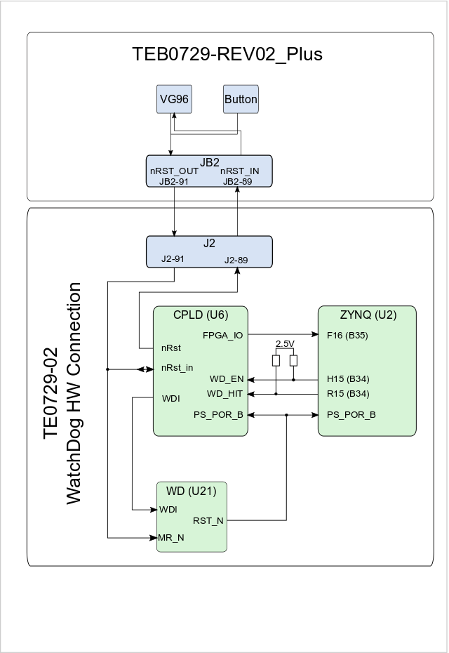 Figure2: Firmware for TEB0729 with modification,
|
B2B Control:
2 Variant available,depends on carrier board connection, see Figure 1 and 2. The swapped signals and Variant 1 nRST_IN pulse limitation are the only different between this tow variants.
Variant 1(Figure 1):
| IOs | Direction | Description |
|---|---|---|
| nRST | in | Main Reset to module |
| nRST_IN | out | Main reset to carrier and PS_POR_B for approx. 1,9 us. |
Variant 2 (Figure 2):
| IOs | Direction | Description |
|---|---|---|
| nRST | out | Main reset to carrier and PS_POR_B |
| nRST_IN | in | Main Reset to module |
1V Power supply:
Reset PS, if 1V drop down. Connected on PCB, controlled by WD SENSE pin.
CPLD Control:
FPGA Control:
Status / GPIO
BOARD_STAT is used as WD restart indicator and as user IO.
| Modus | Condition |
|---|---|
| Slow Blink | If PS_POR_B is low and appr. 30s long after PS_POR_B goes up |
| User defined | appr. 30s long after PS_POR_B goes up and as long as PS_POR_B is high |
Info: On TEB0729, signal is connected to XMOD LED.
Appx. A: Change History and Legal Notices
...
Overview
Content Tools