Page History
...
Storage device name | Content | Notes |
|---|---|---|
User configuration EEPROMs (1x Microchip 24LC128-I/ST, 3x Microchip 24AA025E48T-I/OT) | Not programmed | - |
| USB3.0 HUB Configuration EEPROM (Microchip 24LC128-I/ST) | Not programmed | - |
| Si5338A programmable PLL NVM OTP | Not programmed | - |
Table 12: Initial Delivery State of the flash memories
...
| B2B | I/O Signal Count | LVDS-pairs count | VCCO bank Voltage | Reference Clock Input from FMC Connector | Notes |
|---|---|---|---|---|---|
| J1 | 48 | 24 | FMC_VADJ | - | bank's VREF-pin connected to FMC connector pin J5-H1 (VREF_A_M2C) |
| J3 | 20 | 10 | FMC_VADJ | 1 LVDS clock from FMC connector J5 (pins J5-G2, J5-G3) | - |
| J4 | 92 | 46 | FMC_VADJ | 1 LVDS clock from FMC connectorJ5 (pins J5-H4, J5-H5) | bank's VREF-pin connected to FMC connector pin J5-H1 (VREF_A_M2C) |
Table 23: FMC connector pin-outs of available logic banks of the MPSoC
...
| B2B | Type | Count of MGT Lanes | Schematic Names / Connector Pins | MGT Bank's Reference Clock Inputs from FMC Connector |
|---|---|---|---|---|
| J1 | GTH | 4 GTH lanes | B228_RX3_P, B228_RX3_N, pins J5-A10, J5-A11 B228_RX2_P, B228_RX2_N, pins J5-A6, J5-A7 B228_RX1_P, B228_RX1_N, pins J5-A2, J5-A3 B228_RX0_P, B228_RX0_N, pins J5-C6, J5-C7 | 1 MGT clock (B228_CLK0) from FMC connector |
| J1 | GTH | 4 GTH lanes | B229_RX3_P, B229_RX3_N, pins J5-B12, J5-B13 B229_RX2_P, B229_RX2_N, pins J5-B16, J5-B17 B229_RX1_P, B229_RX1_N, pins J5-A18, J5-A19 B229_RX0_P, B229_RX0_N, pins J5-A14, J5-A15 | 1 MGT clock (B229_CLK0) from FMC connector |
| J1 | GTH | 2 GTH lanes | B230_RX1_P, B230_RX1_N, pins J5-B4, J5-B5 B230_RX0_P, B230_RX0_N, pins J5-B8, J5-B9 | - |
Table 34: FMC connector pin-outs of available MGT lanes of the MPSoC
...
| Clock Signal Schematic Name | FMC Connector Pins | Direction | Clock Source | Notes |
|---|---|---|---|---|
| B228_CLK0 | J5-D4 / J5-D5 | in | FMC Connector J5 | Extern MGT clock |
| B229_CLK0 | J5-B20 / J5-B21 | in | FMC Connector J5 | Extern MGT clock |
| FMCCLK2 | J5-K4 / J5-K5 | out | Carrier Board PLL SI5338A U35, CLK2 | Clock signal to Mezzanine module |
| FMCCLK3 | J5-J2 / J5-J3 | out | Carrier Board PLL SI5338A U35, CLK3 | Clock signal to Mezzanine module |
| B64_L14_P / B64_L14_N | J5-H4 / J5-H5 | in | FMC Connector J5 | LVDS Clock to PL bank |
| B48_L6_P / B48_L6_N | J5-G2 / J5-G3 | in | FMC Connector J5 | LVDS Clock to PL bank |
Table 45: FMC connector pin-outs for reference clock output
...
| Interfaces | I/O Signal Count | Pin schematic Names / FMC Pins | Connected to | Notes |
|---|---|---|---|---|
| JTAG | 5 | FMC_TCK, pin J5-D29 FMC_TMS, pin J5-D33 FMC_TDI, pin J5-D30 FMC_TDO, pin J5- D31 | SC CPLD U17, bank 1 | VCCIO: 3V3SB TRST_L, pin J5-D34 pulled-up to 3V3_PER |
| I²C | 2 | FMC_SCL, pin J5-C30 FMC_SDA, pin J5-C31 | I²C Switch U16 | I²C-lines pulled-up to 3V3_PER |
| Control Lines | 4 | FMC_PRSNT_M2C, pin J5-H2 FMC_PG_C2M, pin J5-D1 (3V3_PER pull-up) FMC_PG_M2C, pin J5-F1 (3V3_PER pull-up) FMC_CLK_DIR, pin J5-B1 (pulled-down to GND) | I²C I/O Expander U38 SC CPLD U39, bank 0 I²C I/O Expander U38 SC CPLD U17, bank 1 | 'PG' = 'Power Good'-signal 'C2M' = carrier to (Mezzanine) module 'M2C' = (Mezzanine) module to carrier |
Table 56: FMC connector pin-outs of available interfaces to the System Controller CPLD
...
| VCCIO Schematic Name | FMC Connector J5 Pins | Notes |
|---|---|---|
| 12V | C35/C37 | extern 12V power supply |
| 3V3_PER | D32/D36/D38/D40/C39 | 3.3V peripheral supply voltage |
| FMC_VADJ | H40/G39/F40/E39 | adjustable FMC VCCIO voltage, supplied by DC-DC converter U8 |
Table 67: Available VCCIO voltages on FMC connector
...
| MIO | Configured as | System Controller CPLD | Notes |
|---|---|---|---|
| 0..12 | Dual QSPI | - | Dual Flash Memory on TE0808 / -03 TE0803 SoM; Bootable |
| 13..23 | SD0: eMMC | - | eMMC Memory U2; Bootable |
| 24, 25 | - | CPLD (U39) MUXED | - |
| 26..29 | - | CPLD (U17 MUXED | Bootable JTAG (PJTAG0) |
| 30 | force reboot after FSBL-PLL config for PCIe | CPLD (U39) MUXED | - |
| 31 | PCIe reset | CPLD (U39) MUXED | - |
| 32 | - | CPLD (U39) MUXED | - |
| 33 | - | CPLD (U39) MUXED | - |
| 34..37 | - | CPLD (U39) MUXED | - |
| 38, 39 | I2C0 | - | - |
| 40 | forwarded to PWRLED_P / LED_P | CPLD (U39) MUXED | - |
| 41 | - | - | - |
| 42, 43 | UART0 | CPLD (U39) MUXED | - |
| 44 | SD_WP to FPGA | CPLD (U39) MUXED | - |
| 45..51 | SD1: SD | - | Bootable MikroSD / MMC Card |
| 52..63 | USB0 | - | - |
| 64..75 | GEM3 | - | Ethernet RGMII |
| 76, 77 | MDC / MDIO | - | Ethernet RGMII |
Table 78: MIO Assignment
Following interfaces are provided by the MIO bank of the Zynq Ultrascale+ MPSoC:
...
The PS GT Bank 505 provides beside the USB3.0 Lane also following interfaces:
- SATA (PS GT bank 505, MGT2 Lane)
- DisplayPort (PS GT bank 505, MGT3 Lane, only TX-pair routed)
- PCI Express (PS GT bank 505, MGT0 Lane)
| Function | MGT Lane | Required Ref Clock | Clock Source | Comment |
|---|---|---|---|---|
| PCIe | PS 0 | 100 MHz | clock signal of SoM's prog. PLL | single lane PCIe connector clock signal routed on carrier board to PCIe connector J1 |
| USB3 | PS 1 | 100 MHz | clock signal of SoM's prog. PLL | clock signal routed on-module, |
| SATA | PS 2 | 150 MHz | On-board oscillator U23 | optional: clock signal of SoM's prog. PLL |
| DP.0 | PS 3 | 27 MHz | clock signal of SoM's prog. PLL | DisplayPort GT SERDES clock signal, |
Table 89: PS GT Lane Assignment
Following block diagram shows the wiring of the MGT Lanes of the PS GT bank 505 to the particular high speed data interfaces:
...
Figure 5: TEBF0808 PS GT Bank 505 Interface
MGT Interfaces SFP+ and FireFly
The TEBF0808 carrier board provides the high speed MGT interface connectors "SFP+" (Enhanced small form-factor pluggable) and Samtec "FireFly". Each of this connectors are capable of data transmission rates up to 10 Gbit/s.
...
Follwowing table contains a brief description of the control and status signals of PCIe interface:
| Signal Schematic Name | FPGA Direction | Description | Logic |
|---|---|---|---|
| WAKE | Input | Link reactivation | Low active |
| PERST | Output | PCI Express reset input | Low active |
| PRSNT1 | Input | Reference pin for PCIe Card lane size | - |
| PRSNT2 | Input | PCI Express ×1 cards | connect to PRSNT1 |
| PRSNT3 | Input | PCI Express ×4 cards | connect to PRSNT1 |
| PRSNT4 | Input | PCI Express ×8 cards | connect to PRSNT1 |
| PRSNT5 | Input | PCI Express ×16 cards | connect to PRSNT1 |
| PCIE_I²C | BiDir | 2-wire PCIE System Management Bus | - |
Table 10: Description of MGT Connectors Control and Status Signals
MGT Interfaces SFP+ and FireFly
The TEBF0808 carrier board provides the high speed MGT interface connectors "SFP+" (Enhanced small form-factor pluggable) and Samtec "FireFly". This connectors are capable of data transmission rates up to 10 Gbit/s with SFP+ and 28 Gbit/s with FireFly.
| Function | MGT Lane | Required Ref Clock | Clock Source | Comment |
|---|---|---|---|---|
| FireFly | MGT Lanes 0..3 | - | clock signal of SoM's prog. PLL | clock signal on-module routed to MGT bank |
| SFP | MGT Lane 2 | 125 / 156.25 MHz | clock signal of SoM's prog. PLL | clock signal routed on carrier board to MGT bank |
| SFP | MGT Lane 3 | 125 / 156.25 MHz | clock signal of SoM's prog. PLL | clock signal routed on carrier board to MGT bank |
Table 11: MGT Lane Assignment
Following block diagram show the wiring of the MGT lanes to the particular interface connectors:
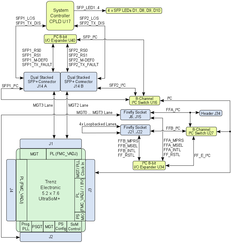
Figure 6: TEBF0808 MGT Interfaces
As shown on the block diagram, the FireFly connector pair J21, J22 provides four reversed looped back MGT lanes. To test any of the on-board MGT lanes or of an extern device, 4 RX/TX differential pairs are bridged on the connector, hence the transmitted data on these MGT lanes flows back to their sources in a loop-back circuit without intentional processing or modification.
Follwowing table contains a brief description of the control and status signals of the MGT lanes incorporating SFP+ and Samtec FireFly connectors:
| Signal Schematic Name | Connector Type | FPGA Direction | Description | Logic |
|---|---|---|---|---|
| SFPx_TX_DISABLE | SFP+ | Output | SFP Enabled / Disabled | Low active |
| SFPx_LOS | SFP+ | Input | Loss of receiver signal | High active |
| SFPx_RS0 | SFP+ | Output | Full RX bandwidth | Low active |
| SFPx_RS1 | SFP+ | Output | Reduced RX bandwidth | Low active |
| SFPx_M-DEF0 | SFP+ | Input | Module present / not present | Low active |
| SFPx_TX_FAULT | SFP+ | Input | Fault / Normal Operation | High active |
| SFPx_I²C | SFP+ | BiDir | 2-wire Serial Interface | - |
| FFx_MPRS | FireFly | Output | depending on connected module | - |
| FFx_MSEL | FireFly | Output | depending on connected module | - |
| FFx_INTL | FireFly | Input | Module interrupt line | - |
| FFx_RSTL | FireFly | Output | Module reset line | - |
| FFx_I²C | FireFly | BiDir | 2-wire Serial Interface | - |
Table 12: Description of MGT Connectors Control and Status Signals
Table 9: MGT Lane Assignment
Following block diagram show the wiring of the MGT lanes to the particular interface connectors:
Figure 6: TEBF0808 MGT Interfaces
As shown on the block diagram, the FireFly connector pair J21, J22 provides four reversed looped back MGT lanes. To test any of the on-board MGT lanes or of an extern device, 4 RX/TX differential pairs are bridged on the connector, hence the transmitted data on these MGT lanes flows back to their sources in a loop-back circuit without intentional processing or modification.
CAN FD Interface and PMOD Connectors
...
| PMOD | Interface | Connected to | Notes |
|---|---|---|---|
| P1 | GPIO | HP Bank of MPSoC (4 I/O's, B65_T0 ... B65_T3), System Controller CPLD U17 (4 I/O's, EX_IO1 ... EX_IO4) | Voltage translation via IC U33 with direction control, only singled-ended signaling possible |
| P2 | I²C | 8-channel I²C Switch U27 | Accessible on MPSoC's I²C interface through I²C switch U27 |
| P3 | I²C | 8-channel I²C Switch U27 | Accessible on MPSoC's I²C interface through I²C switch U27 |
Table 1013: PMOD Pin Assignment
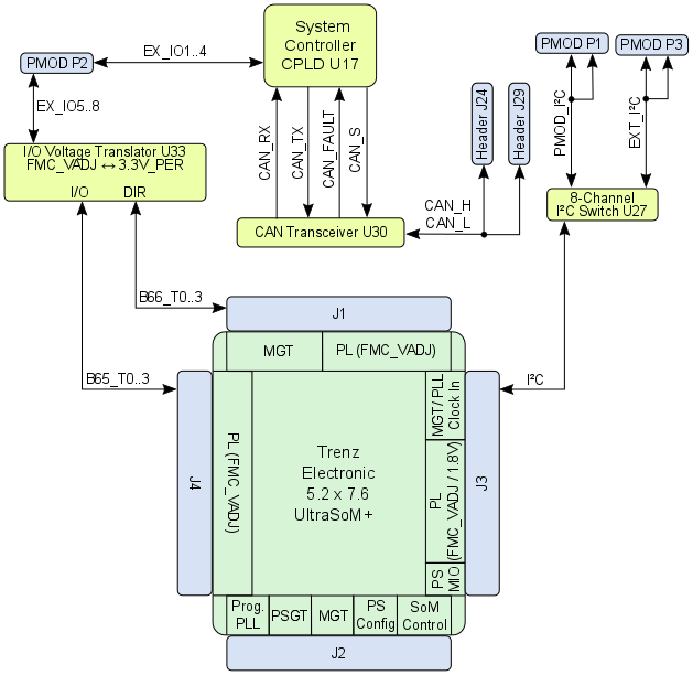
Figure 7: TEBF0808 CAN Interfaces, PMOD
...
| Header | Pin Name | Functionality | Connected to | Notes |
|---|---|---|---|---|
| J10 | Pin 1, HD LED+ | HD LED Anode | SC CPLD U39 | Reset and Power switch-pins are also connected to switch buttons S1 and S2 |
| J9 | Pin 1, PORT1L | Microphone Jack Left Microphone Jack Right Audio Out Jack Left Audio Out Jack Right Jack Detect / Mic in Ground | 24-bit Audio Codec U3 | - |
| J23 | Pin 1, 3V3SB Pin 4, S1 | 3.3V DC Supply PC compatible Beeper | SC CPLD U39 | - |
| J26 | Pin 1, GND | Ground 12V DC Supply RPM PWM | SC CPLD U39 | 4-wire PWM FAN connector |
| J35 | Pin 1, GND | Ground 12V DC Supply RPM PWM | SC CPLD U39 | 4-wire PWM FAN connector |
| J19 | Pin 1, GND | Ground 5V DC Supply | Load Switch Q3 (5V DC) | 2-wire FAN connector Fan off/on switchable by signal 'FAN_FMC_EN' on SC CPLD U39 |
Table 1114: PC compatible Headers
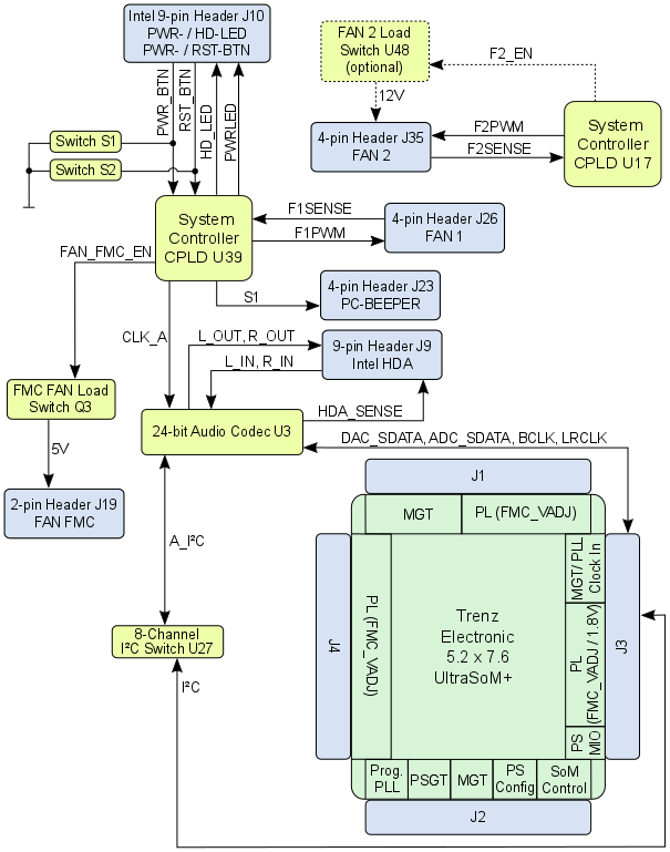
Figure 8: TEBF0808 PC Compatible Headers
...
| Si5338A (U35) Input | Signal Schematic Name | Note |
|---|---|---|
IN1/IN2 | CLK8C_P, CLK8C_N | Clock signal of SoM's prog. PLL |
IN3 | reference clock signal from oscillator SiTime SiT8008BI (U7) | 25.000000 MHz fixed frequency. |
IN4 | pin put to GND | LSB (pin 'IN4') of the default I²C-adress 0x70 not activated. |
IN5/IN6 | pins not connected / put to GND | not used, differential feedback input |
| Si5338A (U35) Output | Signal Schematic Name | Note |
CLK0 A/B | SC_CLK0 | Clock signal to SC CPLD U17 (single-ended signaling) |
CLK1 A/B | SC_CLK1 | Clock signal to SC CPLD U17 (single-ended signaling) |
CLK2 A/B | FMCCLK2_P, FMCCLK2_N | Clock signal routed to FMC connector J5, pins J5-K4 / J5-K5 |
| CLK3 A/B | FMCCLK3_P, FMCCLK3_N | Clock signal routed to FMC connector J5, pins J5-J2 / J5-J3 |
Table 1215: Pin description of PLL clock generator Si5338A
...
Figure 11: Clocking Configuration of TE0808 SoM on TEBF0808 Carrier Board
| Note |
|---|
Si5338 OTP ROM is not programmed by default at delivery, so it is customers responsibility to either configure Si5338 during FSBL or then use SiLabs programmer and burn the OTP ROM with customer fixed clock setup. |
Si5338 OTP can only be programmed two times, as different user configurations may required different setup, TEBF0808 is normally shipped with blank OTP.
For more information Si5338 at SiLabs.
| Note |
|---|
Refer to the TE0808 / TE0803 TRM for the configuration and for the internal routing of the on-module Si5345 10multi-channel PLL clock generator signals to the clock input pins of the MGT banks.Also how to configure the programmable Si5345 PLL clock generator on the mounted TE0808 SoM. |
Oscillators
The TEBF0808 carrier board is equipped several on-board oscillators to provide the Zynq Ultrascale+ MPSoC's PS and PL banks and the on-board peripherals with reference clock-signals:
| Clock Source | Schematic Name | Frequency | Clock Input Destination |
|---|---|---|---|
| SiTime SiT8008BI oscillator, U10 | USB0_RCLK | 52.000000 MHz | USB 2.0 transceiver PHY U9, pin 26 |
| SiTime SiT8008BI oscillator, U13 | ETH_CLK | 25.000000 MHz | Gigabit Ethernet PHY U12, pin 34 |
| SiTime SiT8008BI oscillator, U7 | - | 25.000000 MHz | Quad PLL clock generator U35, pin 3 |
| DSC1123 oscillator, U23 | B505_CLK1 | 150.0000 MHz | PS GT Bank, dedicated for SATA interface |
DSC1123 oscillator, U6 optional, not equipped | B505_CLK0 | 100.0000 MHz | PS GT Bank, dedicated for USB interface |
Silicon Labs 570FBB000290DG, U45 optional, not equipped | B47_L5 (LVDS) | 250.MHz | PL Bank clock capable input pins |
| SiTime SiT8008BI oscillator, U25 | CLK_CPLD | 25.576000 MHz | System Controller CPLD U35, pin 128 |
Table 1316: Reference clock signal oscillators
...
| PHY Pin | Connected to | Notes |
|---|---|---|
| ULPI | PS bank MIO52 ... MIO63 | Zynq Ultrascale+ USB0 MIO pins are connected to the PHY |
| REFCLK | - | 52MHz from on board oscillator (U9) |
| REFSEL[0..2] | - | All pins set to GND selects the external reference clock frequency (52.000000 MHz) |
| RESETB | SC CPLD U17 | Low active USB PHY Reset (pulled-up to PS_1.8V). |
| DP, DM | 4-port USB3.0 Hub U4 | USB2.0 data lane |
| CPEN | - | External USB power switch active-high enable signal |
| VBUS | 5V | Connected to USB VBUS via a series of resistors, see schematic |
| ID | - | For an A-device connect to the ground. For a B-device, leave floating |
Table 1417: USB PHY interface connections
...
| PHY Pin | Connected to | Notes |
|---|---|---|
| MDC/MDIO | PS bank MIO76, MIO77 | - |
| PHY LED0..1 | SC CPLD U17, pin 67,86 | see schematic for details, forwarded to RJ45 GbE MagJack J7 |
| PHY_LED2 / INTn: | SC CPLD U17, pin 85 | Active low interrupt line |
| PHY_CLK125M | SC CPLD U17, pin 70 | 125 MHz Ethernet PHY clock out |
| CONFIG | SC CPLD U17, pin 65 | Permanent logic high |
| RESETn | SC CPLD U17, pin 62 | Active low reset line |
| RGMII | PS bank MIO64 ... MIO75 | Reduced Gigabit Media Independent Interface |
| SGMII | - | Serial Gigabit Media Independent Interface |
| MDI | RJ45 GbE MagJack J7 | Media Dependent Interface |
Table 1518: Ethernet PHY interface connections
...
The I2C bus works internally on-module with reference voltage 1.8V, it is connected to the MPSoC I2C interface via PS MIO bank (pins MIO38, MIO39) configured as master.
| MIO | Signal Schematic Name | Notes |
|---|---|---|
| 38 | I2C_SCL | 1.8V reference voltage |
| 39 | I2C_SDA | 1.8V reference voltage |
Table 1619: MIO-pin assignment of the module's I2C interface
I2C addresses for on-board slave devices are listed in the table below:
There are further I²C interfaces connected to the 8-channel I²C switches U16 and U27, which are provided by connectors with I²C interface. The I²C slave addresses depend on the devices, which are attached to this connectors:
| I²C Slave Devices connected to MPSoC I²C Interface | I²C Switch Position | I²C Slave Address | Schematic Names of I²C Bus Lines | I²C Switch||||||||||||
|---|---|---|---|---|---|---|---|---|---|---|---|---|---|---|---|
| 8-channel I²C switch U16 | - | 0x73 | I2C_SDA / I2C_SCL | ||||||||||||
| 8-channel I²C switch U27 | - | 0x77 | I2C_SDA / I2C_SCL | ||||||||||||
| SC CPLD U39, bank 2, pins 52 (SDA), 50 (SCL) | - | User programmable U160x73 | I2C_SDA / I2C_SCL | - | |||||||||||
| I²C Slave Devices connected to 8-channel I²C | switch U270x77 | I2C_SDA / I2C_SCL | Switch U16 | I²C Switch Position | I²C Slave Address | Schematic Names of I²C Bus Lines | -|||||||||
| On- | moduleboard Quad programmable PLL clock generator | Si5345U35 Si5338 | 0x69 | PLL_SDA / PLL_SCL | U27 | Configuration EEPROM U24 | 0x54 | 0 | 0x70 | MCLK | MEM_SDA / | MEMMCLK_SCL | U16 | Configuration EEPROM U36 | 0x52 | MEM
| 8-bit I²C IO Expander U44 | 1 | 0x26 | SFP_SDA / | MEMSFP_SCL | U16 | ||||||||||
| Configuration EEPROM U41 | 0x51 | MEM_SDA / MEM_SCL | U16 | ||||||||||||
| PCIe Connector J1 | 2 | module dependent | PCIE | Configuration EEPROM U22 | 0x50 | MEM_SDA / | MEMPCIE_SCL | U16 | |||||||
| SFP+ Connector J14A | 3 | module dependent | SFP1 | 8-bit I²C IO Expander U44 | 0x26 | SFP_SDA / | SFPSFP1_SCL | U16 | |||||||
| SFP+ Connector J14B | 4 | module dependent | SFP2 | 24-bit Audio Codec U3 | 0x38 | A_I2C_SDA / | ASFP2_ | I2C_SCL | U27 | ||||||
| Configuration EEPROM U24 | 5 | 0x54 | MEM | USB3.0 Hub configuration EEPROM U5 | 0x51 | USBH_SDA / USBHMEM_SCL | U16 | USB3.0 Hub | 0x60 | ||||||
| Configuration EEPROM U36 | 5 | 0x52 | MEMUSBH_SDA / USBHMEM_SCL | U16 | |||||||||||
| Configuration EEPROM U41 | 5 | 0x51 | 8-bit I²C IO Expander U38 | 0x27 | MEM_SDA / MEM_SCL | U16 | |||||||||
| Configuration EEPROM U22 | 5 | 0x50 | MEM | On-board Quad programmable PLL clock generator U35 Si5338 | 0x70 | MCLK_SDA / MCLKMEM_SCL | U16 | ||||||||
| 8-bit I²C IO Expander | U34U38 | 5 | 0x240x27 | FFMEM_ | E_SDA / | FF_EMEM_SCL | U27 | ||||||||
| FMC Connector J5 | 6 | module dependent | FMC | SC CPLD U17, bank 3, pins 13 (SDA), 14 (SCL) | User programmable | SC_SDA / | SCFMC_SCL | U27 | |||||||
| SC CPLD U39, bank 2, pins 52 (SDA), 50 (SCL) | User programmable | I2C_SDA / I2C_SCL | - |
...
| USB3.0 Hub configuration EEPROM U5 | 7 | 0x51 | USBH_SDA / USBH_SCL |
| USB3.0 Hub | 7 | 0x60 | USBH_SDA / USBH_SCL |
| I²C Slave Devices connected to 8-channel I²C Switch U27 | I²C Switch Position | I²C Slave Address |
|---|
| Schematic Names of I²C Bus Lines |
|---|
| PMOD Connector P1 | 0 | module dependent | PMOD |
| _SDA / |
| PMOD_SCL |
| 24-bit Audio Codec U3 | 1 | 0x38 | A_I2C_SDA / |
| A_I2C_SCL |
| FireFly Connector J15 | 2 | module dependent | FFA_SDA / FFA_SCL |
| FireFly Connector J22 | 3 | module dependent | FFB_SDA / FFB_SCL |
| On-module Quad programmable PLL clock generator Si5345 (TE0808) | 4 | 0x69 | PLL |
| _SDA / |
| PLL_SCL | |||
| SC CPLD U17, bank 3, pins 13 (SDA), 14 (SCL) | 5 | User programmable | SC_SDA / SC_SCL |
| 8-bit I²C IO Expander U34 | 6 | 0x24 | FF_E_SDA / FF_E_SCL |
| PMOD Connector P3 | 7 | module dependent | EXT_SDA / EXT_SCL |
Table 1820: On-board connectorsperipherals' I2C-interfaces overviewdevice slave addresses
Configuration EEPROMs
The TEBF0808 carrier board contains several EEPROMs for configuration and general user purposes. The EEPROMs are provided by Microchip and all have I²C interfaces:
| EEPROM Modell | Schematic Designator | Memory Density | Purpose |
|---|---|---|---|
| 24LC128-I/ST | U24 | 128 Kbit | user |
| 24AA025E48T-I/OT | U36 | 2 Kbit | user |
| 24AA025E48T-I/OT | U41 | 2 Kbit | user |
| 24AA025E48T-I/OT | U42 | 2 Kbit | user |
| 24LC128-I/ST | U5 | 128 Kbit | USB3.0 Hub U4 configuration memory |
Table 1921: On-board configuration EEPROMs overview
...
| DIP-switch S4 | Position ON | Position OFF | Notes |
|---|---|---|---|
| S4-1 | PUDC_B is Low | PUDC_B is HIGH | Internal pull-up resistors during configuration are enabled at ON-position, means I/O's are 3-stated until configuration of the FPGA completes. |
| S4-2 | x | x | not connected |
| S4-3 | SC CPLDs' JTAG enabled | SC CPLDs' JTAG disabled | JTAG interface is enabled on both SC CPLDs, as this CPLDs are configured in a casdaced JTAG chain. |
| S4-4 | DC-DC converter U18 (5V) enabled | DC-DC converter U18 (5V) not manually enabled | In OFF-position, the DC-DC-converter will be still enabled by the Enable-signal of SC CDPD U17 (wired-OR circuit). |
Table 2022: DIP-switch S4 functionality description
...
| S5-1 | S5-2 | S5-3 | S5-4 | Description |
|---|---|---|---|---|
| ON | ON | ON | ON | Default, boot from SD/eMMC, 1.8V FMC VADJ |
| ON | ON | x | x | Boot from microSD, SD or SPI Flash |
| OFF | ON | x | x | Boot from eMMC |
| ON | OFF | x | x | Boot mode PJTAG0 |
| OFF | OFF | x | x | Boot mode main JTAG |
| x | x | x | ON | FMC VADJ = 1.8V |
| x | x | x | OFF | FMC VADJ = 1.2V |
Table 2123: DIP-switch S4 functionality description
...
| LED | Color | Description and Notes |
|---|---|---|
| D4 | green | Status LED, connected to SC CPLD U17 |
| D5 | red | Status LED, connected to SC CPLD U17 |
| D6 | green | Status LED, connected to SC CPLD U39 |
| D7 | red | Status LED, connected to SC CPLD U39 |
| D1 | red | SFP+ interface status LED, connected to SC CPLD U17 |
| D8 | green | SFP+ interface status LED, connected to SC CPLD U17 |
| D9 | red | SFP+ interface status LED, connected to SC CPLD U17 |
| D10 | green | SFP+ interface status LED, connected to SC CPLD U17 |
| D17 | green | LED is on if all USB3.0 and USB 2.0 ports are in the suspend state and is |
Table 2224: On-board LEDs functionality description
...
Xilinx provide a power estimator excel sheets to calculate power consumption. It's also possible to evaluate the power consumption of the developed design with Vivado. See also Trenz Electronic Wiki FAQs also possible to evaluate the power consumption of the developed design with Vivado. See also Trenz Electronic Wiki FAQ.
Power Distribution Dependencies
All on-board voltages of the TEBF0808 are generated out of the extern applied 12V power supply.
There are following dependencies how the initial 12V power supply is distributed to the on-board DC-DC converters, which power up further DCDC converters and the particular on-board voltages:
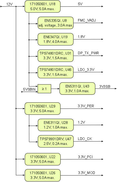
Figure 12: Power Distribution Diagram
| Note |
|---|
Current rating of Samtec Razor Beam™ LSHM B2B connectors is 2.0A per pin (2 adjacent pins powered). |
Power-On Sequence Diagram
...
Following diagram visualizes the connection of the DC-DC converter control signals ('Enable', 'Power-Good') with System Controller CPLD U39, which enables the particular on-board voltages.
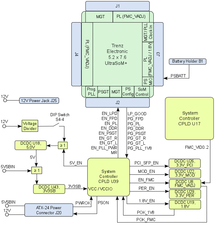
Figure 1213: Power-On Sequence Utilizing DCDC Converter Control Signals
...
The TEBF0808 carrier board manages both the power-on sequence of the mounted TE0808 / TE0803 SoM and the on-board DC-DC converters via System Controller CPLD U39.
The power-on sequence of the TE0808 / TE0803 SoM is managed by utilizing the SoM's DC-DC converter control signals ('Enable', 'Power-Good'), so the DC-DC converters of the SoM dedicated to the particular Power Domains of the Zynq Ultrascale+ MPSoC will be powerer-up in a specific sequence to meet the recommended criteria to power up the Xilinx Zynq Ultrascale+ MPSoC properly.
...
| FMC_VID2 | FMC_VID1 | FMC_VID0 | FMC_VADJ Value |
|---|---|---|---|
| 0 | 1 | 0 | 1.8V |
| 0 | 1 | 1 | 1.5V |
| 1 | 0 | 0 | 1.25V |
| 1 | 0 | 1 | 1.2V |
Table 325: Bit patterns for fixed values of the FMC_VADJ voltage
Note: These pins of the DC-DC converter U8 are hard-wired to initialiy fix the voltage to 1.8V (see schematic).
Power Distribution Dependencies
All on-board voltages of the TEBF0808 are generated out of the extern applied 12V power supply.
There are following dependencies how the initial 12V power supply is distributed to the on-board DC-DC converters, which power up further DCDC converters and the particular on-board voltages:
Figure 13: Power Distribution Diagram
...
values of the FMC_VADJ voltage
Note: These pins of the DC-DC converter U8 are hard-wired to initialiy fix the voltage to 1.8V (see schematic).
B2B connectors
| Include Page | ||||
|---|---|---|---|---|
|
...
| Note |
|---|
| Please check TRM TE0808 / TE0803 and Xilinx datasheet DS925 for complete list of absolute maximum and recommended operating ratings for the mounted TE0808 SoMUltraSoM+. |
Operating Temperature Ranges
...
| Date | Revision | Notes | Link to PCN | Documentation Link |
|---|---|---|---|---|
| - | 04 | current Current available board revision | - | TEBF0808-04 |
| - | 03 | Second production release | - | TEBF0808-03 |
| - | 02 | First production release | - | TEBF0808-02 |
| - | 01 | Prototype | - | - |
...
Overview
Content Tools