Page History
...
The TEC0330 FPGA board is intended to be used as add-on card in a PCIe 2.0 or higher capable host systems, it can not be used as a stand-alone device.
Key Features
...
- Xilinx Virtex-7 FPGA module XC7VX330T-2FFG1157C (commercial temperature range)
- PCI Express 2.0 x8 card with maximum throughput of 4 GB/s
- FMC High Pin Count (HPC) connector
- 8 FPGA MGT lanes available on PCIe interface
- DDR3 SO-DIMM SDRAM socket
- 256-Mbit (32-MByte) Quad SPI Flash memory (for configuration and operation) accessible through:
- FPGA
- JTAG port (SPI indirect, bus width x4)
- External clock input via SMA coaxial connector
- 28 GTH transceivers, each with up to 13.1 Gbit/s data transmission rate
- FPGA configuration through:
- JTAG connector
- SPI Flash memory
- Programmable quad PLL clock generator
- TI LMK04828B ultra low-noise JESD204B compliant clock jitter cleaner
- On-board high-efficiency DC-DC converters
- Up to 202 FPGA I/O pins available on FMC connector (up to 101 LVDS pairs possible)
- System management and power sequencing
- AES bit-stream encryption
- eFUSE bit-stream encryption
...
Additional assembly options are available for cost or performance optimization upon request.
...
Block Diagram
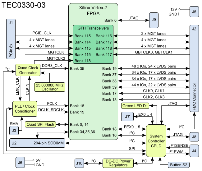
Figure 1: TEC0330-03 Block Diagram.
...
Overview
Content Tools