Page History
...
Table 13: I/O pin description of PLL clock generator Si5338A.
| Page break |
|---|
Ultra low-noise high-performance clock synthesizer
...
The on-board voltages of the TEC0330 FPGA board will be powered - up in order of a determined sequence after the external voltages ' 12V ' on connector J5 and ' 3V3PCI ' on connector J1 are available.
Core voltages and main supply voltages have to reach stable state and their "Power Good"-signals have to be asserted before other voltages like PL bank's I/O voltages can be powered up.
Following diagram clarifies describes the sequence of enabling the particular on-board voltages:
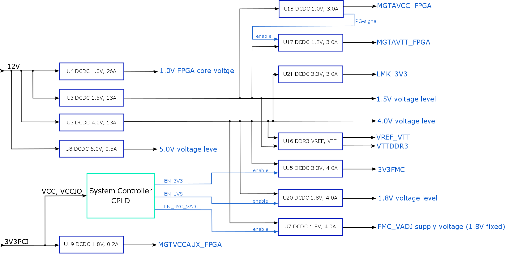
Figure 3: FPGA board TEC0330-03 Power-On sequence diagram.
...
Overview
Content Tools