Page History
...
The Trenz Electronic TE0723 -03 is a Arduino compatible FPGA module based on the Xilinx Zynq XC7Z010 SoC.
...
Additional assembly options are available for cost or performance optimization upon request.
Block Diagram
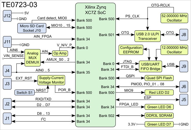
Figure 1: TE0723 block diagram.
Main Components
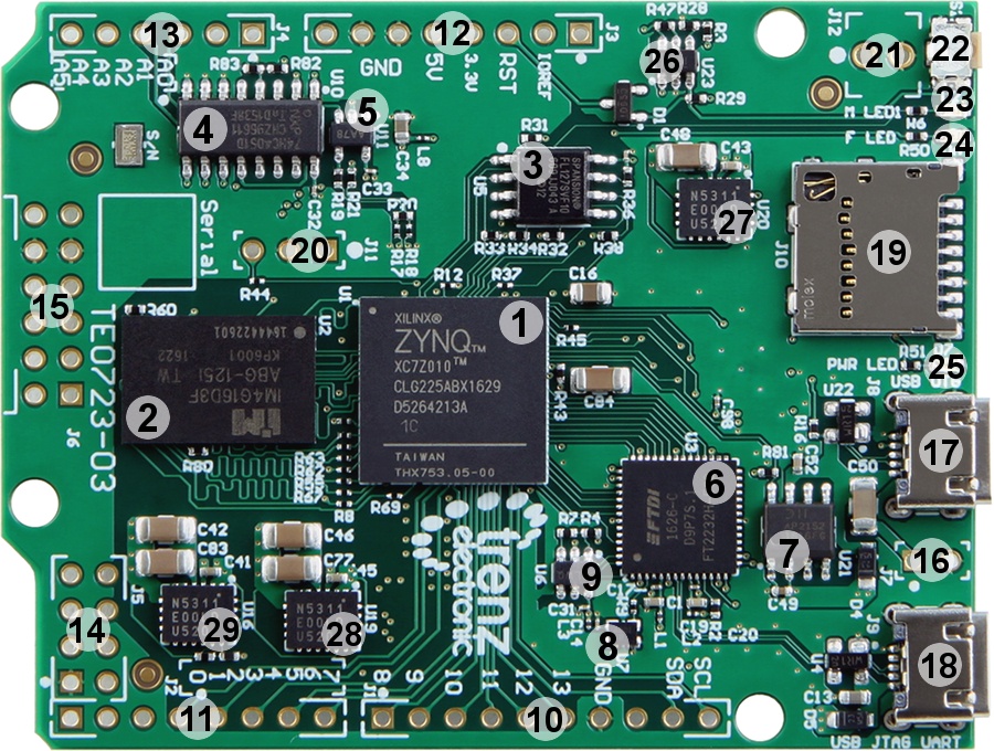
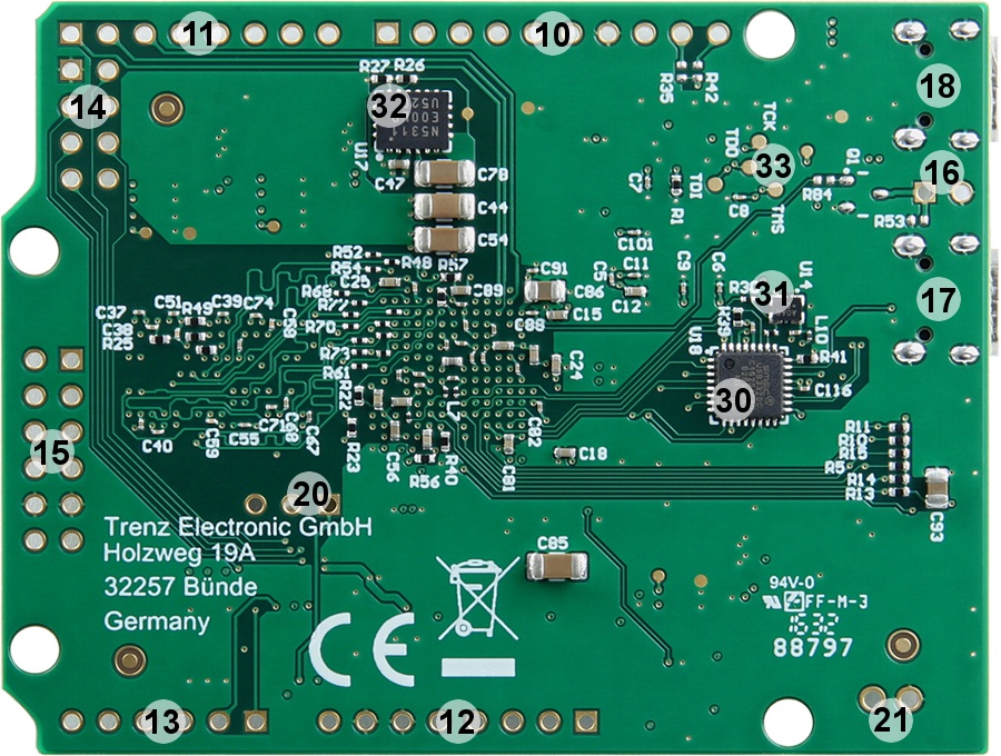
Figure 2: Main components of the TE0723 module.
- Xilinx ZYNQ Zynq XC7Z010 SoC, U1
- 4 Gbit DDR3L 256M x 16 SDRAM, U2
- 16 MByte QSPI Flash memory, U5
High-speed CMOS logic analog multiplexer/demultiplexer, U10
- 1 MHz low-power operational amplifier, U11
- Dual high-speed USB to multipurpose UART/FIFO, U3
- 0.5A dual-channel current-limited power switch, U21
- Low-power programmable oscillator @ 12.000000 MHz, U7
- 2 Kbit Microwire compatible serial EEPROM, U6
- 10-pin header, J1
- 8-pin header, J2
- 10-pin header, J3
- Analog input header, J4
- 2 x 4-pin header, J5
- PMod 2x6 interface header, J6
- USB host mode jumper, J7
- Micro USB 2.0 Type-B receptacle, J8
- Micro USB 2.0 Type-B receptacle, J9
- Micro SD card connector with detect signal, J10
- Analog input select jumper, J11
- 5V supply power input, J12
- Reset switch, S1
- Red LED, D2
- Green LED, D6
- Green LED, D7
- Ultra-low supply-current voltage monitor, U23
1A PowerSoC DC-DC converter (3.3 V), U20
- 1A PowerSoC DC-DC converter (1.8 V, U19
- 1A PowerSoC DC-DC converter (1.35 V), U16
- Hi-speed USB 2.0 ULPI transceiver, U18
- Low-power programmable oscillator @ 52.000000 MHz, U14
- 1A PowerSoC DC-DC converter (1.0 V), U17
- JTAG interface testpoints, TP1-TP4
...
Storage device name | Content | Notes |
|---|---|---|
Quad SPI Flash | Empty |
Table 1: Initial delivery state of programmable devices on the module.
Boot Process
...
Signals, Interfaces and Pins
...
JTAG access to the Xilinx ZYNQ Zynq XC7Z010 SoC is provided through testpoints TP1-T4.
...
| Clock Signal | Frequency | IC | Signal, Pin |
|---|---|---|---|
Processing system (PS) reference clock. | 52.000000 MHz | U1 | PS_CLK, C7 |
USB transceiver reference clock. | 52.000000 MHz | U18 | OTG-RCLK, 26 |
| High-speed USB to multipurpose UART/FIFO oscillator input. | 12.000000 MHz | U3 | OSCI, 3 |
On-board LEDs
| LED | Color | Connected To | Description and Notes |
|---|---|---|---|
| D2 | Red | MIO9, U1 | |
| D6 | Green | Bank 34, U1 | FPGA_LED |
| D7 | Green | 3.3V | PWR_LED |
Power and Power-On Sequence
...
Overview
Content Tools