Page History
| HTML |
|---|
<!--
Template Revision 1.67
(HTML comments will be not displayed in the document, no need to remove them. For Template/Skeleton changes, increase Template Revision number. So we can check faster, if the TRM style is up to date).
--> |
| HTML |
|---|
<!--
General Notes:
If some section is CPLD firmware dependent, make a note and if available link to the CPLD firmware description. It's in the TE shop download area in the corresponding module -> revision -> firmware folder.
--> |
| HTML |
|---|
<!--
General Notes:
Designate all graphics and pictures with a number and a description. For example "Figure 1: TE07xx-xx Block Diagram" or "Table 1: Initial delivery state". "Figure x" and "Table x" have to be formatted to bold.
--> |
| Scroll pdf ignore | |
|---|---|
Table of Contents
|
Overview
| HTML |
|---|
<!--
Wiki Link: Go to Base Folder of the Module or Carrier, for example : https://wiki.trenz-electronic.de/display/PD/TE0712
--> |
| Scroll Only (inline) |
|---|
Refer to http://trenz.org/te0724-info for the current online version of this manual and other available documentation. |
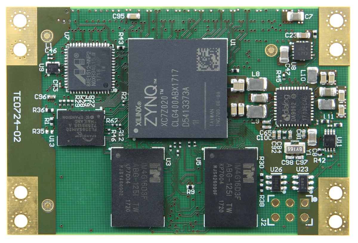
The Trenz Electronic TE0724 is an industrial-grade SoC module based on Xilinx Zynq 7010/7020, which provides a dual core ARM Cortex A9 and a 7-series FPGA logic. It provides a gigabit ethernet transceiver, 1 GByte of DDR3L SDRAM, 64 MByte Flash memory as configration and data storage. It includes strong power regulators for all needed voltages and a robust high-speed connector for in- and outputs. It has a 6 x 4 cm form factor.
Key Features
- Xilinx Zynq XC7Z010-1CLG400I or XC7Z020-1CLG400I
- Dual-core ARM Cortex-A9 MPCore
- Max. 667 MHz
- Shock proof and vibration resistant
- Size 6 x 4 cm
- Plug-On-Modul with 1 × 160 Pin High-Speed connector
- 1 GByte DDR3L SDRAM
- 64 MByte QSPI Flash Speicher
- 1 x GBit Ethernet PHY
- 1 x MAC-Address EEPROM
- 128 KBit EEPROM
- 1 x CAN Transceiver
- On-Board DC/DC-regulators
- Excellent signal integrity due to evenly-spread supply pins
Additional assembly options are available for cost or performance optimization upon request.
Block Diagramm
| Scroll Title | ||||||||||||||||||||||||||||||
|---|---|---|---|---|---|---|---|---|---|---|---|---|---|---|---|---|---|---|---|---|---|---|---|---|---|---|---|---|---|---|
| ||||||||||||||||||||||||||||||
|

Main Components
| Scroll Title | ||||||||||||||||||||||||||||||||||||||||||||||||||||||
|---|---|---|---|---|---|---|---|---|---|---|---|---|---|---|---|---|---|---|---|---|---|---|---|---|---|---|---|---|---|---|---|---|---|---|---|---|---|---|---|---|---|---|---|---|---|---|---|---|---|---|---|---|---|---|
| ||||||||||||||||||||||||||||||||||||||||||||||||||||||
|

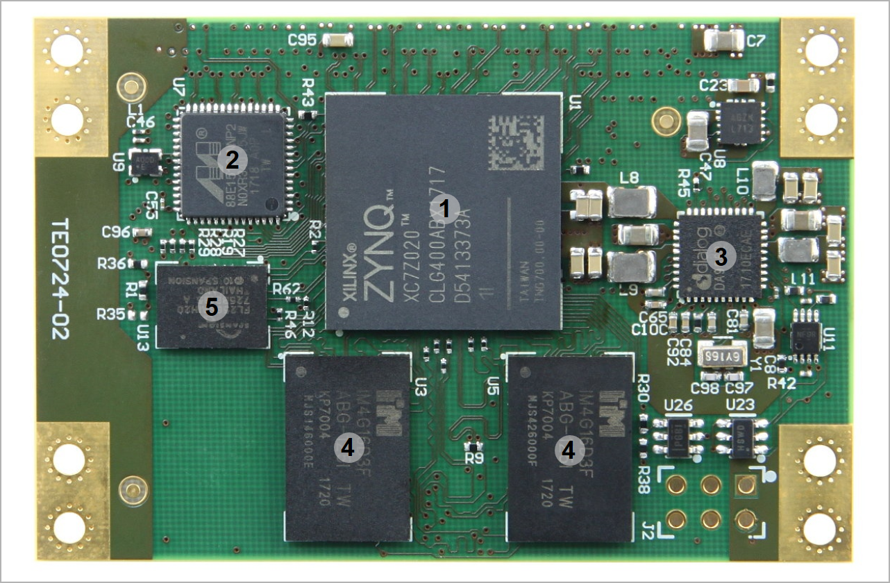
- XILINX ZYNQ XC7Z020-2CLG400C, U1
- Gigabit Ethernet Transceiver Alaska 88E1512, U7
- Power Manager Dialog DA9062, U4
- 1GByte - 2x 4Gbit DDR3L RAM, U3, U5
- 64MByte ISSI SPI Flash IS25LP512M, U13
- 128KByte Serial EEPROM Microchip 24AA, U10
- CAN Transceiver MCP2542FDT, U2
- 160 Pin Samtec B2B Connector ST5-80-1.50-L-D-P-TR, J1
Initial Delivery State
Storage device name | Content | Notes |
|---|---|---|
| ISSI SPI Flash IS25LP512M, U13 | Empty | |
| DA9062, U4 | Programmed | |
| Microchip 24AA128T, U10 | Empty | USER EEPROM |
| Microchip 24AA025E48T, U23 | MAC write protected preprogrammed, User area empty | EEPROM for MAC-Address. |
Table 1: Initial delivery state of programmable devices on the module.
Boot Process
Boot mode is selected via two Mode pins at B2B connector J2. By default the TE0724 supports JTAG and SPI Boot Mode. Connecting a SD Card via B2B connector to MIO Pins (See SD Card Interface) gives the possibility to boot from SD Card. The Mode pins are pulled up at the module.
Boot mode | MODE1 J1-2 | MODE0 J1-4 |
|---|---|---|
| JTAG (cascade) | LOW | LOW |
| invalid | LOW | HIGH |
| SPI | HIGH | LOW |
| SD CARD (not on module) | HIGH | HIGH |
Table 2: Boot mode selection.
Signals, Interfaces and Pins
| HTML |
|---|
<!--
Connections and Interfaces or B2B Pin's which are accessible by User
--> |
Board to Board (B2B) I/Os
I/O signals connected to the SoCs I/O bank and B2B connector:
| Bank | Type | B2B Connector | I/O Signal Count | Bank Voltage | Notes |
|---|---|---|---|---|---|
| 500 | MIO | J1 | 8 I/Os | 3.3V | On-module power supply. |
| 501 | MIO | J1 | 12 I/Os | 1.8V | On-module power supply. |
| 34 | HR | J1 | 32 I/Os or 16 LVDS pairs | 3.3V | On-module power supply. |
| 35 | HR | J1 | 48 I/Os or 24 LVDS pairs | VCCIO_35 | Supplied by the carrier board. |
Table 3: General overview of PL I/O signals connected to the B2B connectors.
All PS MIO banks as well as PL bank 34 are powered by on-module DC-DC power rails. Valid VCCO_35 for PL bank 35 should be supplied via the B2B connector.
For detailed information about the pin out, please refer to the Pin-out Tables.
The configuration of the PS I/Os MIO40 to MIO51 depend on the carrier board peripherals connected to these pins.
| HTML |
|---|
<!--
TO-DO (future):
If Vivado board part files are available for this module, the standard configuration of the MIO pins by using this board part files should be mentioned here. This standard configuration of those pins are also apparent of the on-board peripherals of base-boards related to the module.
--> |
| HTML |
|---|
<!--
MGT lanes should be listed separately, as they are more specific than just general I/Os.
--> |
JTAG Interface
JTAG access to the ZYNQ SoC is provided through B2B connector J1 and testpoints.
JTAG Signal | B2B Connector Pin |
|---|---|
| TCK | J1-147 |
| TDI | J1-151 |
| TDO | J1-145 |
| TMS | J1-149 |
Table 4: JTAG interface signals.
System Controller Pins
Special purpose pins are available for System Controller functions and are routed to the Power Management IC (U4) with the following default configuration:
| Signal Name | Mode | Function | B2B Connector Pin | Configuration |
|---|---|---|---|---|
| RESETREQ | INPUT | Reset request | J1-150 | Aktive LOW, enter reset mode when set low. Pulled up to VIN. |
| ONKEY | INPUT | Power-on key | J1-148 | Debounced edge sensitve power mode manipulator. On/Off with optional long press shutdown, function dependent on register value of NONKEY_PIN, KEY_DELAY. |
| PWR_TP | IN/OUT | Test pin | J1-146 | Enables Power Commander boot mode and supply pin for OTP fusing voltage. |
| PWR_GPIO2 | IN/OUT | J1-143 | ||
| PWR_GPIO2 | IN/OUT | J1-141 |
Table 5: System Controller CPLD I/O pins.
| HTML |
|---|
<!--
For the detailed function of the pins and signals, the internal signal assignment and implemented logic, look to the Wiki reference page SC CPLD of this module or into the bitstream file of the SC CPLD.
Add link to the Wiki reference page of the SC CPLD, if available.
--> |
Quad SPI Interface
Quad SPI Flash (U13) is connected to the Zynq PS QSPI_0 interface via PS MIO bank 500, pins MIO1 ... MIO6.
| MIO | Signal Name | U14 Pin |
|---|---|---|
| 1 | SPI_CS | C2 |
| 2 | SPI_DQ0/MIO2 | D3 |
| 3 | SPI_DQ1/MIO3 | D2 |
| 4 | SPI_DQ2/MIO4 | C4 |
| 5 | SPI_DQ3/MIO5 | D4 |
| 6 | SPI_SCK/MIO6 | B2 |
Table 6: Quad SPI interface signals and connections.
SD Card Interface
There is no physical SD Card slot on the module. Three different interface options are possible at a carrier via the PS MIO 10 to 15 or 40 to 45 or 46 to 51 plus additional MIOs for SD Card Detect and Write Protect as well as SD Card Power Controls. For details compare Xilinx UG585-Zynq-7000-TRM Table 2-4.
Ethernet Interface PHY
The TE0724 is equipped with a Marvell Alaska 88E1512 Gigabit Ethernet PHY (U7) connected to PS Ethernet GEM0. The I/O Voltage is fixed at 1.8V for HSTL signaling. The reference clock input of the PHY is supplied from an on-board 25.000000 MHz oscillator (U9), the 125MHz output clock signal CLK_125MHZ is connected to the PL IO_L11P_T1_SRCC_34.
| PHY Pin | PS bank 501 | B2B | Notes |
|---|---|---|---|
| MDC/MDIO | MIO52/MIO53 | - | |
| LED0 | - | J1-10 | |
| LED1 | - | J1-12 | |
| LED2/Interrupt | - | - | not connected |
| CONFIG | - | - | connected to 1.8V (VDDO), PHY Address = 1 |
| RESETn | MIO39 | - | |
| RGMII | MIO16..MIO27 | - | |
| SGMII | - | - | not connected |
| MDI | - | J1-7,9,13,15,19,21,25,27 |
Table 7: Ethernet PHY connections.
CAN PHY
A felxible data rate CAN Transceiver is provided by a Microchip MCP2542FDT.
| PHY Pin | PL bank 34 | B2B | Notes |
|---|---|---|---|
| TX/RX | IO_L1P/IO_L1N | - | |
| CAN_L / CAN_H | - | J1-1 / J1-3 |
Table 8: CAN PHY connections.
I2C Interface
On-board I2C devices are connected to PS MIO28 (SCL) and MIO29 (SDA). I2C addresses for on-board devices are listed in the table below:
| I2C Device | 7bit I2C Address | Notes |
|---|---|---|
| MAC EEPROM, U23 | 0x53 | 1.8V |
| USER EEPROM, U10 | 0x50 | 1.8V |
| Power Management U4 | 0x58 / 0x59 | 3.3V |
| J1 | - | J1-142 SDA, J1-144 SDL at 3.3V |
Table 9: I2C slave device addresses.
On-board Peripherals
| HTML |
|---|
<!--
Components on the Module, like Flash, PLL, PHY...
--> |
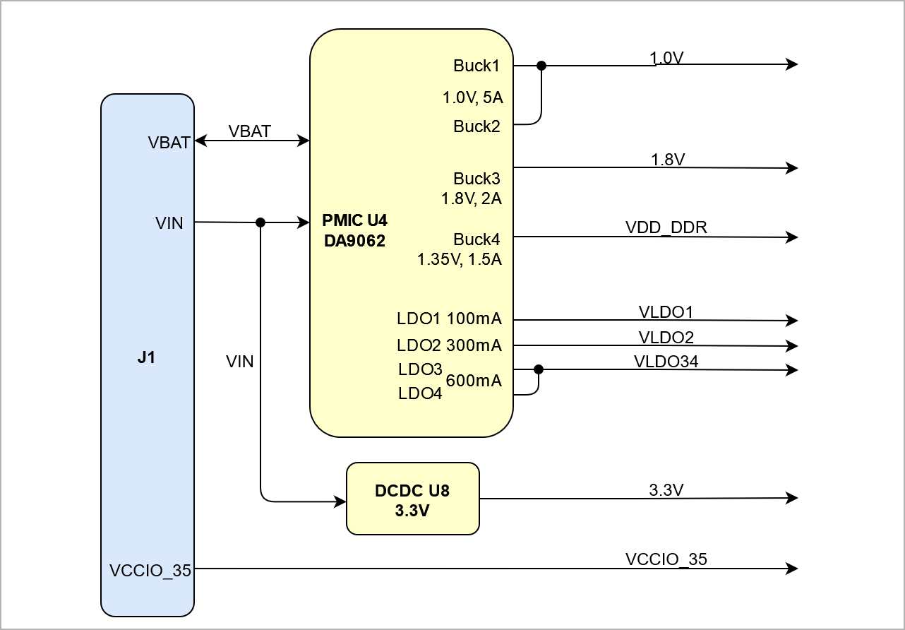
Power Management IC
The power management IC (U4) is provided by dialog Semiconductors (DA9062). It controls the power-on sequencing of the various power rails. It is preprogrammed and accessible via I2C address 0x58 / 0x59. For a detailed description of the configurable power management IC please refer to the datasheet of dialog semicondutor DA9062.
| HTML |
|---|
<!--
Put in link to the Wiki reference page of the firmware of the SC CPLD.
--> |
DDR Memory
By default TE0724 module has 2 DDR3L SDRAM chips arranged into 32-bit wide memory bus providing total of 1 GBytes of on-board RAM. Different memory sizes are available optionally.
Quad SPI Flash Memory
On-board QSPI flash memory (U13) on the TE0724-04 is a ISSI IS25LP512M with 512 Mbit (64 MByte) storage capacity. This non volatile memory is used to store initial FPGA configuration. Besides FPGA configuration, remaining free flash memory can be used for user application and data storage. All four SPI data lines are connected to the FPGA allowing x1, x2 or x4 data bus widths. Maximum data rate depends on the selected bus width and clock frequency used.
| Note |
|---|
SPI Flash QE (Quad Enable) bit must be set to high or FPGA is unable to load its configuration from flash during power-on. By default this bit is set to high at the manufacturing plant. |
MAC Address EEPROM
A Microchip 24AA025E48 serial EEPROM (U23) contains a globally unique 48-bit node address, which is compatible with EUI-48(TM) specification. The device is organized as two blocks of 128 x 8-bit memory. One of the blocks stores the 48-bit node address and is write protected, the other block is available for application use. It is accessible over I2C bus with slave device address 0x53.
| Note |
|---|
Max. I2C Speed for 24AA025E48 EEPROM is 100kHz. |
USER EEPROM
A Microchip 24AA128T serial EEPROM (U10) is available for e.g. module identification and user Data. The device has 128Kbit memory with max 64 bytes page write capability. It is accessible over I2C bus with slave device address 0x50.
| Note |
|---|
Max. I2C Speed for 24AA128T EEPROM is 100kHz. |
Oscillators
The module has following reference clock signals provided by on-board oscillators and external source from carrier board:
| Clock Source | Schematic Signal | Frequency | Clock Destination |
|---|---|---|---|
| SiTime SiT8008BI oscillator, U9 | ETH_XTAL | 25.000000 MHz | XTAL_IN, U7 ETH PHY |
| SiTime SiT8008AI oscillator, U6 | PS_CLK | 33.333333 MHz | PS_CLK_500, Bank 500 |
Table10 : Reference clock signals.
On-board LEDs
| LED | Color | Connected to | Description and Notes |
|---|---|---|---|
| D1 | Green | PS MIO7 | User LED. |
| D2 | Green | PL IO_L3P_T0_34 | User LED. |
| D3 | Red | PL IO_L4N_T0_34 | User LED. |
Table 11: On-board LEDs.
Pin Header
Optional assembled Pin Header J2 can be used for PMIC In-System Programming.
Pin | Signal | B2B |
|---|---|---|
| J2-1 | VIN | J1-154, J1-156, J1-158, J1-160 |
| J2-2 | GND | |
J2-3 | I2C_SCL | J1-142 |
| J2-4 | I2C_SDA | J1-144 |
| J2-5 | ONKEY | J1-148 |
| J2-6 | PWR_TP | J1-146 |
Table 12: Optional assembled Pin Header.
Power and Power-On Sequence
| HTML |
|---|
<!--
If power sequencing and distribution is not so much, you can join both sub sections together
--> |
Power Consumption
The maximum power consumption of a module mainly depends on the design running on the FPGA.
Xilinx provide a power estimator excel sheets to calculate power consumption. It's also possible to evaluate the power consumption of the developed design with Vivado. See also Trenz Electronic Wiki FAQ.
| Power Input | Typical Current |
|---|---|
| VIN | TBD* |
Table 13: Typical power consumption.
* TBD - To Be Determined soon with reference design setup.
Power supply with minimum current capability of ...A for system startup is recommended.
The on-board voltages of the TE0724 SoC module will be powered-up in order of a determined sequence after the external voltages VIN is available and nONKEY is asserted.
| Warning |
|---|
| To avoid any damage to the module, check for stabilized on-board voltages should be carried out (i.e. power good and enable signals) before powering up any SoC's I/O bank voltages VCCO_x. All I/Os should be tri-stated during power-on sequence. |
Power Distribution Dependencies
DCDC U8 component is either TPS82140 (2 A) or MUN12A (3 A) depending on the variant.
| Scroll Title | ||||||||||||||||||||||||||||||
|---|---|---|---|---|---|---|---|---|---|---|---|---|---|---|---|---|---|---|---|---|---|---|---|---|---|---|---|---|---|---|
| ||||||||||||||||||||||||||||||
|
See Xilinx data sheet for additional information. User should also check related base board documentation when intending base board design for TE0724 module.
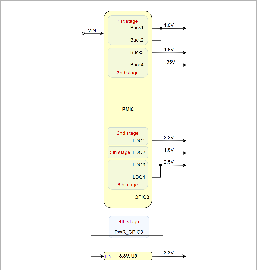
Power-On Sequence
The TE0724 SoM meets the recommended criteria to power up the Xilinx Zynq MPSoC properly by keeping a specific sequence of enabling the on-board DC-DC converters dedicated to the particular functional units of the Zynq chip and powering up the on-board voltages. For a detailed description of the configurable Power Management IC please refer to the datasheet of dialog semicondutor DA9062.
Following diagram clarifies the sequence of enabling the particular on-board voltages, which will power-up in ascending order as listed in the blocks of the diagram:
| Scroll Title | ||||||||||||||||||||||||||||||
|---|---|---|---|---|---|---|---|---|---|---|---|---|---|---|---|---|---|---|---|---|---|---|---|---|---|---|---|---|---|---|
| ||||||||||||||||||||||||||||||
|
Power Rails
Power Rail Name | B2B JM1 Pins | Direction | Notes |
|---|---|---|---|
| VIN | 154, 156, 158,160 | Input | Main supply voltage from the carrier board. |
| VCCIO_35 | 54 | Input | PL Bank 35 supply voltage. |
| VLDO1 | 83 | Output | 3.3V (100mA) |
| VLDO2 | 94 | Output | 1.8V (300mA) |
| VLDO34 | 53 | Output | 2.5V (600mA) |
| 3.3V | 43, 74 | Output | Additional module on-board 3.3V voltage supply (2 A or 3 A variant dependent). |
| 1.0V | - | Buck1 & Buck2 of U4. | |
| 1.8V | 63 | Output | Buck3 of U4. |
| VDD_DDR | - | DDR supply voltage powered by Buck4 of U4. | |
VBAT | 152 | Output/Input | Battery charger (out) and supply for RTC and 32kHz crystal (in). |
Table 14: Module power rails.
Current rating of theSamtec connector is 1.6A per pin (1 pin powered per row).
Bank Voltages
Bank | Schematic Name | Voltage | Voltage Range |
|---|---|---|---|
| 500 MIO | 3.3V | 3.3V | - |
| 501 MIO | 1.8V | 1.8V | - |
| 502 DDR3 | VDD_DDRV | 1.35V | - |
| 34 HR | 3.3V | 3.3V | - |
| 35 HR | VCCIO_35 | User | 1.2V to 3.3V |
Table 15: Module PL I/O bank voltages.
Board to Board Connectors
| Page properties | ||||
|---|---|---|---|---|
| ||||
|
| Include Page | ||||
|---|---|---|---|---|
|
Variants Currently In Production
| HTML |
|---|
<!--
Set correct link to the overview table of the product on english and german, if not available, set
https://shop.trenz-electronic.de/de/Produkte/Trenz-Electronic/
https://shop.trenz-electronic.de/en/Products/Trenz-Electronic/
--> |
| Trenz shop TE0724 overview page | |
|---|---|
| English page | German page |
Technical Specifications
Absolute Maximum Ratings
Parameter | Min | Max | Units | Reference Document |
|---|---|---|---|---|
VIN supply voltage | -0.3 | 5.5 | V | da9062_3v4.pdf |
Storage temperature | -40 | 85 | °C | - |
Table 18: Module absolute maximum ratings.
| Note |
|---|
| Assembly variants for higher storage temperature range are available on request. |
Recommended Operating Conditions
| Parameter | Min | Max | Units | Reference Document |
|---|---|---|---|---|
| VIN supply voltage (variant "-Z" with MUN12A for U8) | 4.5 | 5.5 | V | |
| VIN supply voltage (all other variants) | 3.6 | 5.5 | V | |
| Operating temperature | -40 | 85 | °C |
Table 19: Module recommended operating conditions.
| Note |
|---|
| Please check Xilinx datasheet ... for complete list of absolute maximum and recommended operating ratings. |
Operating Temperature Ranges
Commercial grade: 0°C to +70°C.
Extended grade: 0°C to +85°C.
Industrial grade: -40°C to +85°C.
Module operating temperature range depends also on customer design and cooling solution. Please contact us for options.
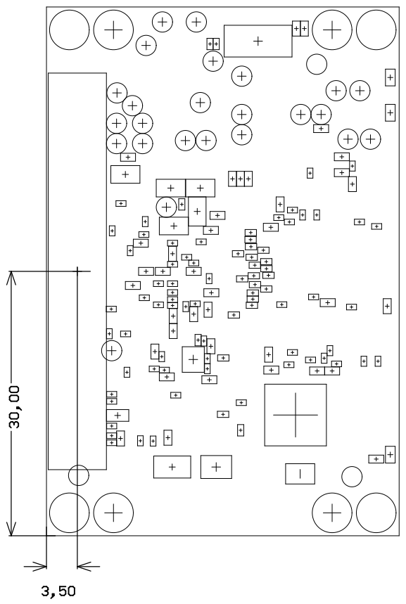
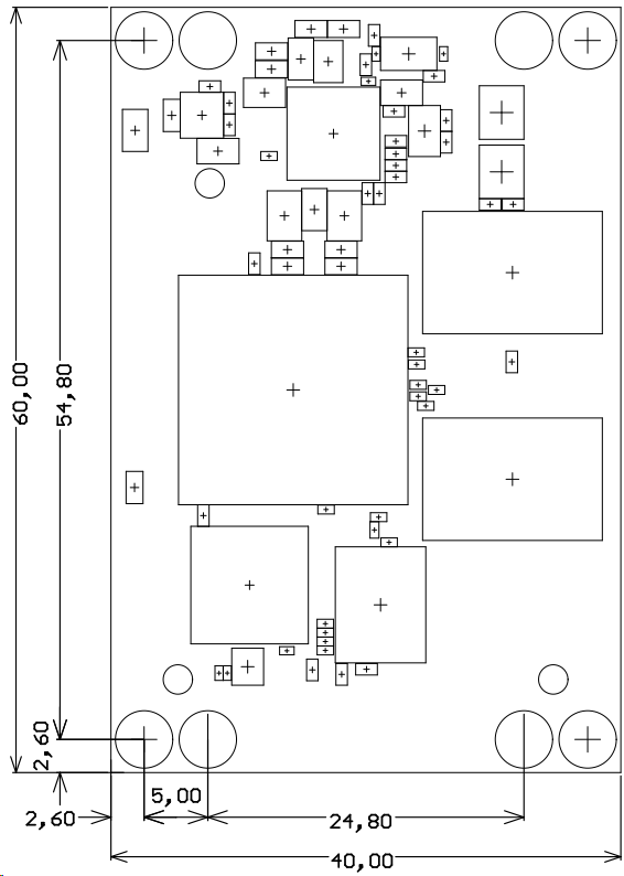
Physical Dimensions
Module size: 60 mm × 40 mm. Please download the assembly diagram for exact numbers.
Mating height with standard connectors: 5.0 mm.
PCB thickness: 1.6 mm.
Highest part on PCB: approx. 1.6 mm. Please download the step model for exact numbers.
All dimensions are given in millimeters.
| Scroll Title | ||
|---|---|---|
| ||
  |
Revision History
Hardware Revision History
| Date | Revision | Notes |
|---|---|---|
| 2020-11-05 | 04 | Changed DDR3, Flash, see PCN |
| 2019-03-12 | 03 | changed 3.3V DCDC |
| 02A | Electrical same as REV 02. | |
| 02 | First production release | |
| - | 01 | Prototypes |
Table 20: Module hardware revision history.
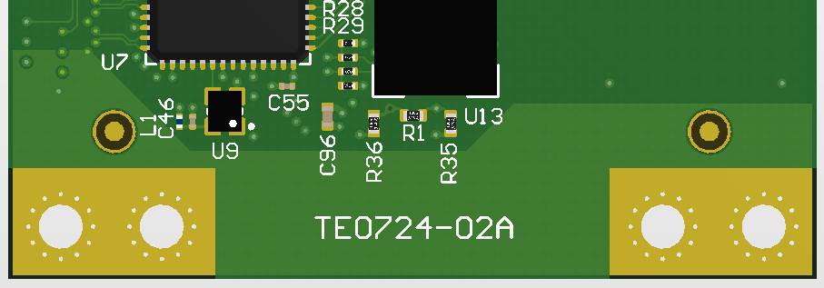
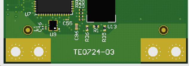
Hardware revision number can be found on the PCB board together with the module model number separated by the dash.
| Scroll Title | ||
|---|---|---|
| ||
|
Document Change History
| HTML |
|---|
<!--
Generate new entry:
1.add new row below first
2.Copy "Page Information Macro(date)" Macro-Preview, Metadata Version number, Author Name and description to the empty row. Important Revision number must be the same as the Wiki document revision number
3.Update Metadata = "Page Information Macro (current-version)" Preview+1 and add Author and change description.
--> |
Date | Revision | Contributors | Description | ||||||||||||||||||||||||||
|---|---|---|---|---|---|---|---|---|---|---|---|---|---|---|---|---|---|---|---|---|---|---|---|---|---|---|---|---|---|
|
|
|
| ||||||||||||||||||||||||||
| 2020-11-17 | v.58 | Martin Rohrmüller |
| ||||||||||||||||||||||||||
| 2019-10-31 | v.56 | Martin Rohrmüller |
| ||||||||||||||||||||||||||
| 2019-10-30 | v.55 | John Hartfield |
| ||||||||||||||||||||||||||
2019-06-27 | v.54 | Martin Rohrmüller |
| ||||||||||||||||||||||||||
2019-06-11 | v.53 | Guillermo Herrera |
| ||||||||||||||||||||||||||
2019-03-29 | v.51 | Martin Rohrmüller |
| ||||||||||||||||||||||||||
2018-11-20 | v.44 | John Hartfiel |
| ||||||||||||||||||||||||||
2018-10-10 | v.43 | John Hartfiel |
| ||||||||||||||||||||||||||
2018-10-09 | v.42 | Martin Rohrmüller |
| ||||||||||||||||||||||||||
2018-10-01 | v.41 | Martin Rohrmüller |
| ||||||||||||||||||||||||||
2018-09-21 | v.39 | Martin Rohrmüller |
| ||||||||||||||||||||||||||
2018-07-20 | v.37 | John Hartfield |
| ||||||||||||||||||||||||||
2018-07-06 | v.34 | Martin Rohrmüller |
| ||||||||||||||||||||||||||
| --- | all |
|
|
Table 21: Document change history.
Disclaimer
| Include Page | ||||
|---|---|---|---|---|
|


Overview
Content Tools