Page History
| HTML |
|---|
<!-- Template Revision 1.64 (HTML comments will be not displayed in the document, no need to remove them. For Template/Skeleton changes, increase Template Revision number. So we can check faster, if the TRM style is up to date). --> |
| Scroll Ignore |
|---|
Download PDF version of this document. |
| Scroll pdf ignore | |
|---|---|
Table of Contents
|
Overview
| Scroll Only (inline) |
|---|
Refer to https://wiki.trenz-electronic.de/display/DRAFT/TE0723+TRM for downloadable version of this manual and additional technical documentation of the product. |
Key Features
- Xilinx Zynq XC7Z010 SoC
- Dual ARM Cortex A9
- 512 MByte DDR3L SDRAM
- 16 MByte quad SPI Flash memory
- Hi-speed USB2.0 ULPI transceiver
- 23 FPGA I/O's available on board-to-board connectors
- Micro SD Card socket with card detect signal
- Micro USB OTG
- On-board USB JTAG and UART
- RGB LED (connected to PL I/O)
- "Done" LED (inverted polarity)
- CERN Open Hardware Licence 1.2
Additional assembly options are available for cost or performance optimization upon request.
Block Diagram
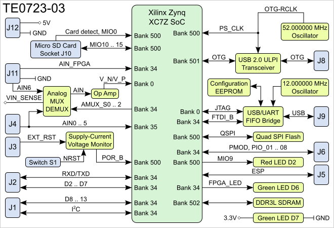
Figure 1: TE0723 block diagram.
Main Components
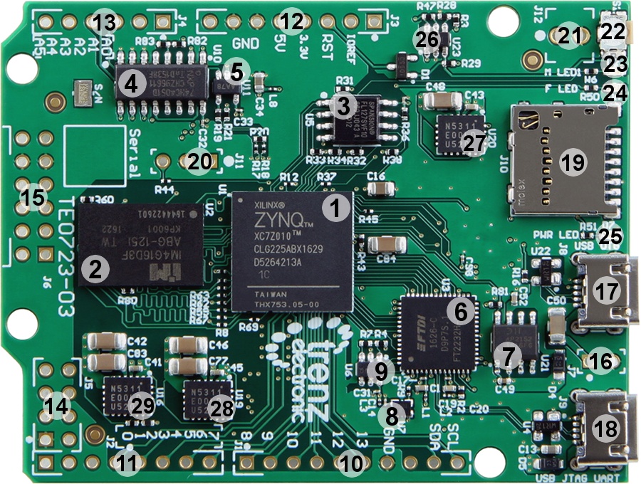
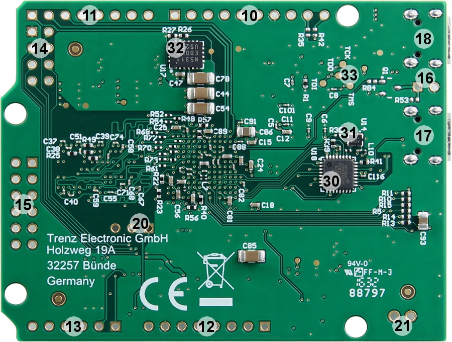
Figure 2: Main components of the TE0723 module.
- Xilinx Zynq XC7Z010 SoC, U1
- 4 Gbit DDR3L 256M x 16 SDRAM, U2
- 16 MByte quad SPI Flash memory, U5
High-speed CMOS logic analog multiplexer/demultiplexer, U10
- 1 MHz low-power operational amplifier, U11
- Dual high-speed USB to multipurpose UART/FIFO, U3
- 0.5A dual-channel current-limited power switch, U21
- Low-power programmable oscillator @ 12.000000 MHz, U7
- 2-Kbit Microwire compatible serial EEPROM, U6
- 10-pin header, J1
- 8-pin header, J2
- 10-pin header, J3
- Analog input header, J4
- 2 x 4-pin header, J5
- PMod 2x6 interface header, J6
- USB host mode jumper, J7
- Micro USB 2.0 Type-B receptacle, J8
- Micro USB 2.0 Type-B receptacle, J9
- Micro SD card connector with detect signal, J10
- Analog input select jumper, J11
- 5V supply power input, J12
- Reset switch, S1
- Red LED, D2
- Green LED, D6
- Green LED, D7
- Ultra-low supply-current voltage monitor, U23
1A PowerSoC DC-DC converter (3.3 V), U20
- 1A PowerSoC DC-DC converter (1.8 V, U19
- 1A PowerSoC DC-DC converter (1.35 V), U16
- Hi-speed USB 2.0 ULPI transceiver, U18
- Low-power programmable oscillator @ 52.000000 MHz, U14
- 1A PowerSoC DC-DC converter (1.0 V), U17
- JTAG interface testpoints, TP1-TP4
Initial Delivery State
Storage device name | IC | Content | Notes |
|---|---|---|---|
Quad SPI Flash | U5 | Empty | |
| Microwire serial EEPROM | U6 | Empty |
Table 1: Initial delivery state of programmable devices on the module.
Boot Process
The 7 boot mode strapping pins on the TE0723 module are set to boot the system from quad SPI Flash only. For additional information refer to the TE0723 schematic and Xilinx UG585 Zynq-7000 All Programmable SoC Technical Reference Manual section "Boot Mode Pin Settings".
You may also refer to this TE0723 reference design for some Boot Process tips.
Signals, Interfaces and Pins
I/O Signals
Overview of the Zynq SoC's PS/PL banks I/O signals connected to the external connectors:
| Bank | Type | Connector | Signal Count | Voltage | Notes |
|---|---|---|---|---|---|
| 34 | HR | J1 | 8 | 3.3V | D8 .. 13, SDA, SCL |
| 34 | HR | J2 | 8 | 3.3V | D2 .. 7, RXD, TXD |
| 34 | HR | J6 | 8 | 3.3V | PIO01 .. PIO08 |
| 35 | HR | J4 | 6 | 3.3V | AIN0 .. 5 |
| 35 | HR | J5 | 1 | 3.3V | ESP_GPIO2 |
| 500 | MIO | J10 | 7 | 3.3V | SDCARD |
| 501 | MIO | J5 | 4 | 3.3V | ESP_RXD, ESP_TXD, ESP_GPIO0, MOD_RST |
Table 2: Overview of the Zynq SoC's PS/PL banks I/O signals.
JTAG Interface
JTAG access to the Xilinx Zynq XC7Z010 SoC is provided through FTDI USB/UART FIFO bridge connected to the J9 Micro USB connector.
Quad SPI Interface
Quad SPI Flash (U5) is connected to the Zynq PS QSPI0 interface via PS MIO bank 500, pins MIO1 ... MIO6.
| Zynq SoC's MIO | Signal Name | U5 Pin |
|---|---|---|
| 1 | SPI0_CS | 1 |
| 2 | SPI0_DQ0/MIO2 | 5 |
| 3 | SPI0_DQ1/MIO3 | 2 |
| 4 | SPI0_DQ2/MIO4 | 3 |
| 5 | SPI0_DQ3/MIO5 | 7 |
| 6 | SPI0_SCK | 6 |
Table 3: Quad SPI interface signals and connections.
SD Card Interface
TE0723 module has on-board 3.3V SD Card socket (J10) with card detect switch wired to the SoC PS MIO bank 500.
| Zynq SoC's Pin | Connected To | Signal Name |
|---|---|---|
| MIO0 | J10-9 | Card detect switch |
| MIO10 | J10-7 | DAT0 |
| MIO11 | J10-3 | CMD |
| MIO12 | J10-5 | CLK |
| MIO13 | J10-8 | DAT1 |
| MIO14 | J10-1 | DAT3 |
| MIO15 | J10-2 | CD/DAT3 |
Table 4: SD card socket signals.
USB Interface
| Zynq SoC's Pin | Connected To | Signal Name |
|---|---|---|
| MIO28 | U18-7 | OTG-DATA4 |
| MIO29 | U18-31 | OTG-DIR |
| MIO30 | U18-29 | OTG-STP |
| MIO31 | U18-2 | OTG-NXT |
| MIO32 | U18-3 | OTG-DATA0 |
| MIO33 | U18-4 | OTG-DATA1 |
| MIO34 | U18-5 | OTG-DATA2 |
| MIO35 | U18-6 | OTG-DATA3 |
| MIO36 | U18-1 | OTG-CLK |
| MIO37 | U18-9 | OTG-DATA5 |
| MIO38 | U18-10 | OTG-DATA6 |
| MIO39 | U18-13 | OTG-DATA7 |
Table 5: USB interface.
ESP Wi-Fi Interface
Interface for the ESP8266 Wi-Fi module is provided through connector J5.
| Zynq SoC's Pin | Connected To | Signal Name |
|---|---|---|
| MIO48 | J5-2 | ESP_TXD |
| MIO49 | J5-7 | ESP_RXD |
| MIO52 | J5-6 | MOD_RST |
| MIO53 | J5-3 | ESP_GPIO0 |
Table 6: ESP8266 Wi-Fi module interface.
I2C Interface
I2C interface pins from the Zynq SoC PL bank 34 are connected to the connector J1. There are no on-board I2C slave devices.
| Zynq SoC's Pin | Connected To | Signal Name |
|---|---|---|
| R13 | J1-9 | SDA |
| P13 | J1-10 | SCL |
Table 7: Zynq SoC I2C interface.
On-board Peripherals
DDR Memory
TE0723 module has up to 512-MBytes of DDR3L SDRAM arranged into 32-bit wide memory bus providing total of 1 GBytes of on-board RAM. Different memory sizes are available optionally.
Quad SPI Flash Memory
On-board quad SPI Flash memory S25FL127S (U5) is used to store initial FPGA configuration. Besides FPGA configuration, remaining free flash memory can be used for user application storage. All four SPI data lines are connected to the Zynq SoC's PS, allowing x1, x2 or x4 data bus widths. Maximum data rate depends on the bus width and clock frequency used.
Dual High-speed USB to Multipurpose UART/FIFO
FT2232H...
High-speed USB ULPI PHY
Hi-speed USB ULPI PHY (U18) is provided with USB3320 from Microchip. The ULPI interface is connected to the Zynq SoC's PS USB0 via MIO28..39, bank 501 (see also section). The I/O voltage is fixed at 3.3V and PHY reference clock input is supplied from the on-board 52.000000 MHz oscillator (U14).
Microwire Serial EEPROM
U36AA56BT-I/OT...
High-Speed Analog Multiplexer
Digitally controlled analog switch TI CD74HC4051...
Low-power Operational Amplifier
The Microchip Technology Inc. MCP6001...
Oscillators
The module has following reference clock signals provided by on-board oscillators:
| Source | Signal | Frequency | Destination | Pin Name | Notes |
|---|---|---|---|---|---|
| U14 | PS_CLK | 52.000000 MHz | U1 | PS_CLK_500 | Zynq SoC PS subsystem main clock. |
| U14 | OTG-RCLK | 52.000000 MHz | U18 | REFCLK | USB3320C PHY reference clock. |
| U7 | OSCI | 12.000000 MHz | U3 | OSCI | FT2232H oscillator input. |
Table 8: Reference clock signals.
On-board LEDs
There are three LEDs on-board TE0723:
| LED | Color | Connected To | Description and Notes |
|---|---|---|---|
| D2 | Red | MIO9, U1 | User LED. |
| D6 | Green | U1, bank 34 pin G14 | FPGA_LED |
| D7 | Green | 3.3V | PWR_LED, power-on LED. |
Table 9: On-board LEDs.
Power and Power-On Sequence
Power Supply
5V power can be supplied by the external power supply through connector J12 or via USB connection to the host system through USB connector J8 or J9. Minimum current capability of 1A for external power supply is recommended.
Power Consumption
Power consumption is to be determined by the user and depends on SoC's FPGA design and connected hardware.
Power-On Sequence
There is no specific power-on sequence, system will power-up itself if 5V is present either through J8, J9 or J12.
Variants Currently in Production
| Module Variant | Xilinx Zynq SoC | DDR3L SDRAM | ARM Cores | PL Cells | LUTs | Flip-Flops | Block RAM | DSP Slices |
|---|---|---|---|---|---|---|---|---|
| TE0723-02 | XC7Z010-1CLG225C | 128 MBytes | Dual-core | 28K | 17,6K | 35,2K | 2.1 MBytes | 80 |
| TE0723-03M | XC7Z010-1CLG225C | 512 MBytes | Dual-core | 28K | 17,6K | 35,2K | 2.1 MBytes | 80 |
| TE0723-03-07S-1C | XC7Z007S-1CLG225C | 512 MBytes | Single-core | 23K | 14,4K | 28,8K | 1.8 MBytes | 66 |
Table 10: Module variants.
Technical Specifications
Absolute Maximum Ratings
Parameter | Min | Max | Units | Reference Document |
|---|---|---|---|---|
VIN supply voltage | -0.5 | 3.6 | V | Xilinx datasheet DS187. |
Storage temperature | -40 | +85 | °C |
Table 11: TE0723 module absolute maximum ratings.
Recommended Operating Conditions
| Parameter | Min | Max | Units | Reference Document |
|---|---|---|---|---|
| Supply voltage | 1.14 | 3.465 | V | Xilinx datasheet DS187. |
Table 12: TE0723 module recommended operating conditions.
| Note |
|---|
| Assembly variants for higher storage temperature range are available on request. |
Physical Dimensions
Module size: 68.58 mm × 53.34 mm. Please download the assembly diagram for exact numbers.
PCB thickness: 1.6 mm.
Highest part on PCB: approx. 4 mm. Please download the step model for exact numbers.
Please note that two different units are used on the figures below, SI system millimeters (mm) and imperial system thousandths of an inch(mil). To convert mils to millimeters and vice versa use formula 100mil's = 2,54mm.
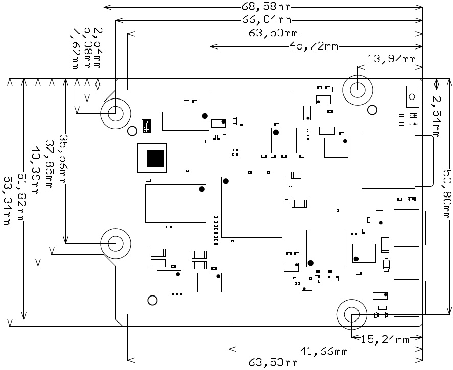
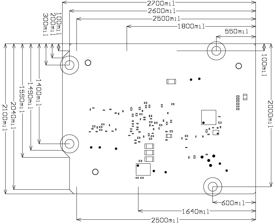
Figure 3: TE0723 module physical dimensions.
Operating Temperature Ranges
Commercial grade: 0°C to +70°C.
Industrial grade: -40°C to +85°C.
Operating temperature range depends also on customer design and cooling solution. Please contact us for options.
Revision History
Hardware Revision History
| Date | Revision | Notes | PCN | Documentation Link |
|---|---|---|---|---|
| 2016-07-15 | 03 | Click to see PCN. | TE0723-03 | |
2015-11-06 | 02 | TE0723-02 | ||
01 |
|
Table 13: TE0723 hardware revision history.
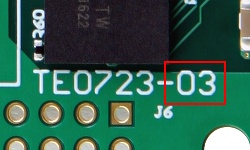
Hardware revision number is printed on the PCB board together with the module model number separated by the dash.
Document Change History
Date | Revision | Contributors | Description | ||||||||
|---|---|---|---|---|---|---|---|---|---|---|---|
| Jan Kumann | Initial document. |
Table 14: Document change history.
Disclaimer
| Include Page | ||||
|---|---|---|---|---|
|
Overview
Content Tools