Page History
...
Additional assembly options are available for cost or performance optimization upon request.
Block Diagram
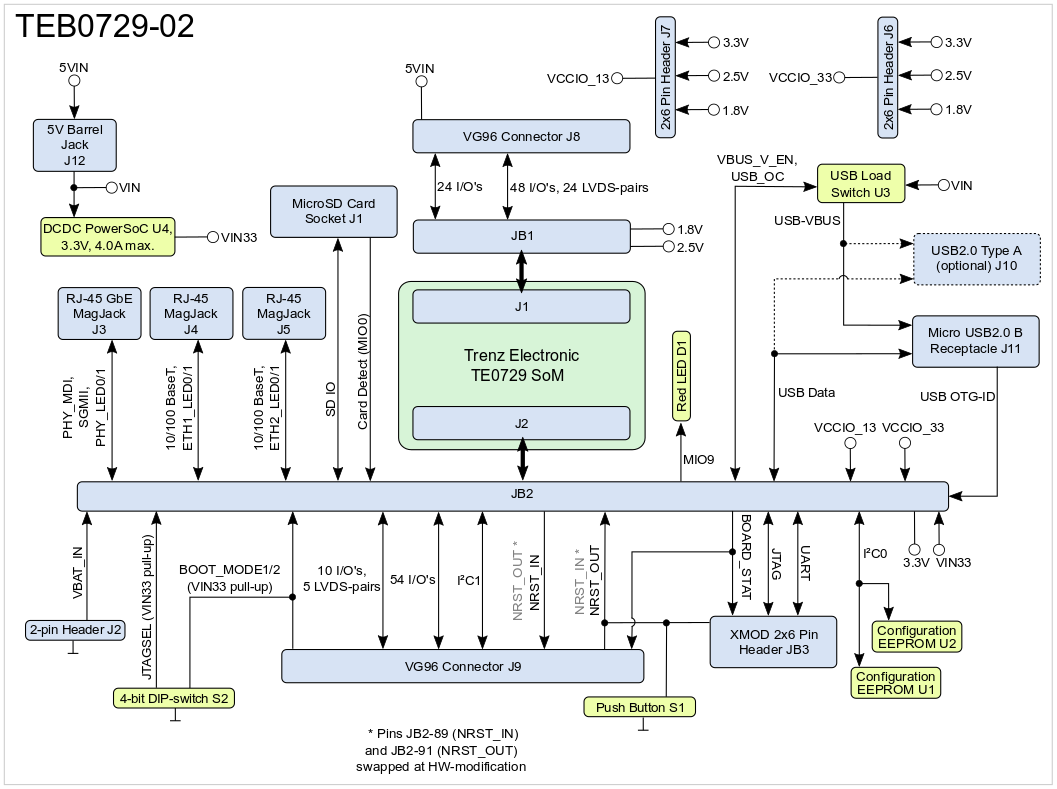
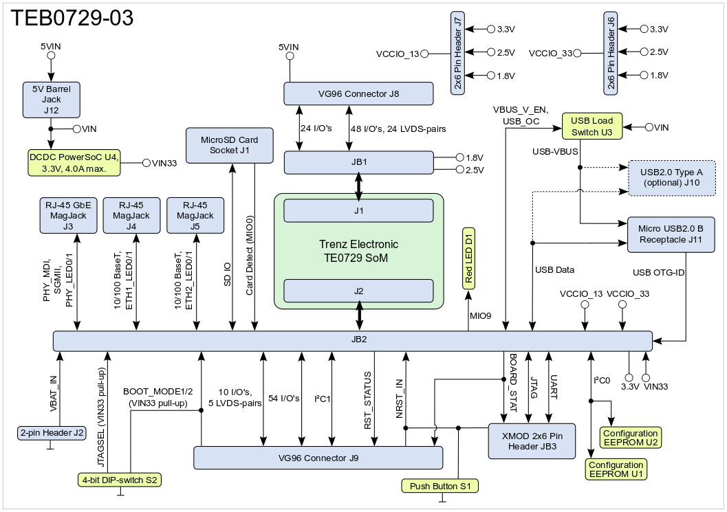
Figure 1: TEB0729-02 block diagram.
...
| B2B Connector | Interfaces | Count of IO's | Notes |
|---|---|---|---|
| JB1 | User IO | 24 single ended | - |
| 48 single ended or 24 differential | - | ||
| JB2 | User IO | 54 single ended | - |
| 10 single ended or 5 differential | - | ||
| I²C | 2 | - | |
| SD IO | 7 | - | |
| UART | 2 | - | |
| USB2.0 | 6 | - | |
| 2x 10/100-BaseT Ethernet | 1412 | - | |
| GbE MDI and SGMII | 14 | - | |
| JTAG | 4 | - |
...
| VG96 Connector | Control Signals and Interfaces | Count of IO's | Notes |
|---|---|---|---|
| J8 | User IO | 24 single ended | - |
| 48 single ended or 24 differential | - | ||
| J9 | User IO | 54 single ended | - |
| 10 single ended or 5 differential | - | ||
| 'NRST_IN', 'NRSTRST_OUTSTATUS', pins J9-A29, J9-B30 | 2SoM reset signals 1) | These pins are dedicated to the specific Reset-functionality of the TE0729 SoM. | |
| 'BOARD_STAT', pins J9-B32 | 1 | - | |
| 'BOOT_MODE1', 'BOOT_MODE2', pins J9-C31, J9-C32 | 2 | Binary bootmode code of SoM | |
| I²C, pins J9-A30, J9-A31 | 2 | I²C1 interface of module | |
| GbE SGMII | 4 | SGMII interface of on-module GbE PHY |
Table 3: General overview of PL I/O signals, SoM's interfaces and control signals connected to the VG96 connectors.
HW-modification Concerning Reset-Signals
1) The pins with the schematic net names 'NRST_IN' (JB2-89) and 'NRST_OUT' (JB2-91) are swapped as part of a HW-modification to rework the Reset-signals of the Carrier-Board in conjunction with the TE0729 SoM.
Refer to the SC CPLD documentation, section "Watchdog" to get further detailed information about the Reset-functionality of the Carrier Board and SoM before and after the HW-modification and the required SC CPLD firmware revision of the TE0729 SoM for each version of the SoMinterfaces and control signals connected to the VG96 connectors.
JTAG Interface
JTAG access to the mounted SoM is provided through B2B connector JB2 and is also routed to the XMOD header JB3. With the TE0790 XMOD USB2.0 to JTAG adapter, the Zynq chip on the mounted SoM can be programed via USB2.0 interface.
...
| 10/100-BaseT PHY Signal Schematic Name | B2B | Connected to | Notes | ||||
|---|---|---|---|---|---|---|---|
| ETH1_RX_P | JB2-26 | J4-3 | - | ||||
| ETH1_RX_N | JB2-28 | J4-6 | - | ||||
| ETH1_TX_P | JB2-20 | J4-1 | - | ||||
| ETH1_TX_N | JB2-22 | J4-2 | - | ||||
| ETH1_CTREF | JB2-30 | J4-4, J4-5 | Centre Tap Reference point | ETH1_LED0 | JB2-34 | Yellow MegJack J4 LED | - |
| ETH1_LED1 | JB2-32 | Green MegJack J4 LED | - | ||||
| ETH2_RX_P | JB2-8 | J5-3 | - | ||||
| ETH2_RX_N | JB2-10 | J5-6 | - | ||||
| ETH2_TX_P | JB2-2 | J5-1 | - | ||||
| ETH2_TX_N | JB2-4 | J5-2 | - | ETH2_CTREF | JB2-18 | J5-4, J5-5Centre Tap Reference point | |
| ETH2_LED0 | JB2-16 | Yellow MegJack J5 LED | - | ||||
| ETH2_LED1 | JB2-14 | Green MegJack J5 LED | - |
...
| JB3 pin | Signal Schematic Net Name | B2B | Note |
|---|---|---|---|
| C (pin 4) | TCK | JB2-119 | - |
| D (pin 8) | TDO | JB2-117 | - |
| F (pin 10) | TDI | JB2-115 | - |
| H (pin 12) | TMS | JB2-113 | - |
| A (pin 3) | USART0_TX | JB2-96 | - |
| B (pin 7) | USART0_RX | JB2-94 | - |
| E (pin 9) | BOARD_STAT | JB2-112 | also connected to VG96 connector pin J9-B32 |
| G (pin 11) 2) | NRST_IN 2) | JB2-89 | also connected to VG96 connector pin J9-A29 |
Table 12: XMOD header signals and connections. 2) Swapped at HW-Modification with signal 'NRST_OUT' in board-revision 2and connections. 2) Pin connected to push button S1 on XMOD FTDI JTAG Adapter
When using XMOD FTDI JTAG Adapter TE0790, the adapter-board's VCC and VCCIO will be sourced by the Carrier Board. Set the DIP-switch with the setting:
...
| Module Variant | Operating Temperature | USB Socket | Temperature Range |
|---|---|---|---|
| TEB0729-0203-A | -40°C to +125°C | USB2.0 Type A socket fitted | Industrial |
| TEB0729-0203-B | -40°C to +125°C | Micro USB2.0 B socket fitted | Industrial |
...
| Date | Revision | Notes | PCN | Documentation Link |
|---|---|---|---|---|
| - | 01 |
| - | TEB0729-01 |
| - | 02 |
| - | TEB0729-02 |
| - | 03 |
| - | TEB0729-03 |
Table 28: Module hardware revision history.
...
Date | Revision | Contributors | Description | ||||||||
|---|---|---|---|---|---|---|---|---|---|---|---|
| Ali Naseri |
| |||||||||
2017-10-27 | v.14 | Ali Naseri |
|
...
Overview
Content Tools