Page History
...
Figure 2: TE0706-02 Carrier Board.
- Samtec Razor Beam™ LSHM-150 B2B connector, JB1
- Samtec Razor Beam™ LSHM-150 B2B connector, JB3
- Samtec Razor Beam™ LSHM-130 B2B connector, JB2
- 6-pin header J26, for selecting PL I/O-bank voltage
- 6-pin header J27, for selecting PL I/O-bank voltage
- Micro USB2.0 Type B Connector J12 (Device or OTG mode)
- JTAG/UART header, JX1 ('XMOD FTDI JTAG Adapter'-compatible pin-assignment)
- User LED D1 (green)
- User LED D2 (red)
- SFP+ Connector, J1
- 50-pin header soldering-pads J17, for access to PL I/O-bank pins (LVDS-pairs possible)
- 50-pin header soldering-pads J20, for access to PL I/O-bank pins (LVDS-pairs possible)
- 16-pin header soldering-pads J3, JTAG/UART header ('XMOD FTDI JTAG Adapter'-compatible pin-assignment)
- 10-pin header soldering-pads J4, for access to SoM's SDIO-port, if available
...
| On-board Pin Header | Control Signals and Interfaces | Count of I/O's | Notes |
|---|---|---|---|
| J17 | User I/O | 42 single ended or 21 differential | - |
| J20 | User I/O | 42 single ended or 21 differential | - |
| J3 | JTAG | 4 | - |
| SoM control signals | 2 | 'RESIN', 'BOOTMODE' | |
| MGT reference input clock | 1 differential pair | AC decoupled on-board (100 nF capacitatorcapacitor) | |
| MIO | 2 | user IO (configurable as UART for example) | |
| J4 | SD IO | 6 | 3.3V and 1.8V voltage level available on header |
...
On the TEBA0841 carrier board is a SFP+ connector J1 (board-rev. 01: Molex 74441-0001). The connector is embedded into a SFP cage J2 (board-rev. 01: Molex 74737-0009).
The differential RX-/TX - data - lanes are connected to B2B - connector JB2, the control-lines are connected to module's IO-pins on B2B-connector JB1 (MIO0-bank-pins in standard TE module's pin-assignment).
On this SFP+ connector, at both 4 x 5 SoMs TE0741 and TE0841 MGT-lane 3 is accessible.
to B2B connector JB1 and are assigned to MIO-bank pins of the mounted SoM.
The pin-assignment of the SFP connector is in detail as fellows:
| SFP+ pin | Pin Schematic Name | B2B | FPGA Direction | Description | Note |
|---|---|---|---|---|---|
| Transmit Data + (pin 18) | MGT_TX3_P | JB2-26 | Output | SFP+ transmit data differential pair | - |
| Transmit Data - (pin 19) | MGT_TX3_N | JB2-28 | Output | - | |
| Receive Data + (pin 13) | MGT_RX3_P | JB2-25 | Input | SFP+ receive data differential pair | - |
| Receive Data - (pin 12) | MGT_RX3_N | JB2-27 | Input | - | |
| Receive Fault (pin 2) | MIO10 | JB1-96 | Input | Fault / Normal Operation |
| High active logic |
| Receive disable (pin 3) |
| 1) | SFP0_TX_DIS | not connected |
| Output | SFP Enabled / Disabled |
| Low active logic | ||||
| MOD-DEF2 (pin 4) | MIO13 | JB1-98 | Input | Module present / not present |
| Low active logic | |||||
| MOD-DEF1 (pin 5) | MIO12 | JB1-100 | Output | 2-wire Serial Interface clock | 3.3V pull-up |
| on-board | |||||
| MOD-DEF0 (pin 6) | MIO11 | JB1-94 | BiDir | 2-wire Serial Interface data | 3.3V pull-up on-board |
| RS0 (pin 7) | SFP0_RS0 |
| not connected | Output | Full RX bandwidth |
| Low active logic | ||||
| LOS (pin 8) | MIO0 | JB1-88 | Input | Loss of receiver signal |
| High active logic | |
| RS1 (pin 9) | SFP0_RS1 |
| not connected | Output | Reduced RX bandwidth |
| Low active logic |
Table 1: SFP+ connector pin-assignment.
1) Important: For proper operation, a wire patch to GND is done at recently delivered boards. Connect to GND, if not done. See PCB drawing below:
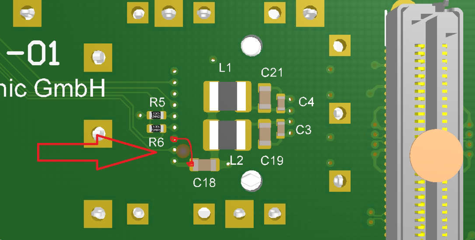
Figure 3: PCB wire patch for SFP+ connector.
Looped-Looped-backed MGT-Lanes on B2B Connector JB1 and JB2
...
The MGT lane pins are bridged on-board as fellows, if 4 x 5 SoM TE0741 is mounted on carrier board:
| MGT Lane | B2B TX Differential Pair | B2B RX Differential Pair | B2B Pins Bridged |
|---|---|---|---|
| MGT-lane 0 | JB2-8 (MGT_TX0_N) JB2-10 (MGT_TX0_P) | JB2-7 (MGT_RX0_N) JB2-9 (MGT_RX0_P) | JB2-7 to JB2-8 JB2-9 to JB2-10 |
| MGT-lane 1 | JB2-14 (MGT_TX1_N) JB2-16 (MGT_TX1_P) | JB2-13 (MGT_RX1_N) JB2-15 (MGT_RX1_P) | JB2-13 to JB2-14 JB2-15 to JB2-16 |
| MGT-lane 2 | JB2-20 (MGT_TX2_N) JB2-22 (MGT_TX2_P) | JB2-19 (MGT_RX2_N) JB2-21 (MGT_RX2_P) | JB2-19 to JB2-20 JB2-21 to JB2-22 |
| MGT-lane 7 | JB1-3 (MGT_TX7_P) JB1-5 (MGT_TX7_N) | JB1-9 (MGT_RX7_P) JB1-11 (MGT_RX7_N) | JB1-3 to JB1-9 JB1-5 to JB1-11 |
| MGT-lane 6 | JB1-15 (MGT_TX6_P) JB1-17 (MGT_TX6_N) | JB1-21 (MGT_RX6_P) JB1-23 (MGT_RX6_N) | JB1-15 to JB1-21 JB1-17 to JB1-23 |
Table 2: Looped-backed MGT-lanes for mounted 4 x 5 SoM TE0741.
...
Following table describes the signals and interfaces of the XMOD header JX1 and pin header J3:
| Pin Schematic Name | XMOD Header JX1 Pin | Header J3 Pin | B2B | Note |
|---|---|---|---|---|
| TCK | C (pin 4) | 4 | JB3-100 | - |
| TDO | D (pin 8) | 8 | JB3-98 | - |
| TDI | F (pin 10) | 10 | JB3-96 | - |
| TMS | H (pin 12) | 12 | JB3-94 | - |
| MIO15 | A (pin 3) | 3 | JB1-86 | UART-TX (transmit line) |
| MIO14 | B (pin 7) | 7 | JB1-91 | UART-RX (receive line) |
| BOOTMODE | E (pin 9) | 9 | JB1-90 | usually |
| 'JTAGSEL' on TE 4 x 5 SoMs | ||||
| RESIN | G (pin 11) | 11 | JB3-17 | SoM Reset pin |
| CLK0_N | - | 15 | JB2-32 | AC decoupled on-board (100 nF |
| capacitor) | ||||
| CLK0_P | - | 16 | JB2-34 | AC decoupled on-board (100 nF |
| capacitor) |
Table 10: JTAG/UART header signals and connections.
When using XMOD FTDI JTAG Adapter TE0790, the adapter-board's VCC and VCCIO will be sourced by the mounted SoM's 'VCCJTAG' (pin JB2-92).on-boards 3.3V supply voltage. Set the DIP-switch with the setting:
| XMOD DIP-switches | Position |
|---|---|
| Switch 1 | ON |
| Switch 2 | OFF |
| Switch 3 | OFF |
| Switch 4 | ONOFF |
Table 11: XMOD adapter board DIP-switch positions for voltage configuration.
...
| HTML |
|---|
<!-- Components on the Module, like Flash, PLL, PHY... --> |
4-bit DIP-switch
Table below describes DIP-switch S1 settings for configuration of the mounted SoM:
...
Boot mode configuration, if supported by SoM. (Depends also on SoM's SC-CPLD firmware).
...
Usually used to enable/disable FPGA core-voltage supply. (Depends also on SoM's SC CPLD firmware).
Note: Power-on sequence will be intermitted if S1-4 is set to OFF and if functionality is supported by SoM.
On-board LEDs
The on-board LEDs are available to the user and can be used to indicate system status and activities:
| LED | Color | Pin Schematic Name | B2B Connector | Description and Notes |
|---|---|---|---|---|
| D1 | Green | MIO9 | JB1-92 | available to user |
| D2 | Red | RLED | JB3-90 | available to user |
Figure 3: On-board LEDs
VCCIO Selection Jumper
On the TEBA0841 carrier board different VCCIO configurations can be selected by the jumper J26 and J27.
TE 4 x 5 Modules have a standard assignment of PL-bank I/O voltages on their B2B connectors, which will be fed with I/O voltage from base-board.
Base-board PL-bank I/O Voltages | B2B Pins | Standard Assignment of PL-bank I/O Voltages on TE 4x5 Modules |
|---|---|---|
| VCCIOA | JB1-10, JB1-12 | VCCIOA (JM1-9, JM1-11) |
| VCCIOD | JB2-8, JB2-10 | VCCIOD (JM2-7, JM2-9) |
Table 5: Base-board PL-bank I/O voltages VCCIOA and VCCIOD
...
Figure 3: User DIP-switch S1
...
| Note |
|---|
Note: The corresponding PL-bank I/O -bank supply- voltages of the 4 x 5 SoM to the selectable base-board voltages VCCIOA , VCCIOB and VCCIOC VCCIOD are depending on the mounted 4 x 5 SoM and varying in order of the used model. Refer to the SoM's schematic for information about the specific pin assignments on module's B2B-connectors regarding the PL-bank I/O -bank supply- voltages and to the 4 x 5 Module integration Guide for VCCIO voltage options. |
The Carrier Board VCCIO for the PL I/O-banks of the mounted SoM are selectable by the jumpers J10, J11 and J12.
Following table describes how to configure the VCCIO of the SoM's PL I/O-banks with jumpers:
...
Following table describes how to configure the base-board supply-voltages by jumpers:
Base-board PL-bank I/O Voltages | VCCIOA | VCCIOD |
|---|---|---|
| 1.8V | J26:1-2 | J27:1-2 |
| 2.5V | J26:3-4 | J27:3-4 |
| 3.3V | J26:5-6 | J27:5-6 |
Table 6: Configuration of base-board supply-voltages via jumpers. Jumper-Notification: 'Jx: 1-2' means pins 1 and 2 are connected, 'Jx: 3-4' means pins 3 and 4 are connected, and so on.
| Note |
|---|
Take care of the VCCO voltage ranges of the particular PL IO-banks (HR, HP) of the mounted SoM, otherwise damages may occur to the FPGA. Therefore, refer to the TRM of the mounted SoM to get the specific information of the voltage ranges. It is recommended to set and measure the PL IO-bank supply-voltages before mounting of TE 4 x 5 module to avoid failures and damages to the functionality of the mounted SoM. |
Power and Power-On Sequence
| HTML |
|---|
<!--
If power sequencing and distribution is not so much, you can join both sub sections together
--> |
Power Consumption
The maximum power consumption of the Carrier Board depends mainly on the mounted SoM's FPGA design running on the Zynq device.
Xilinx provide a power estimator excel sheets to calculate power consumption. It's also possible to evaluate the power consumption of the developed design with Vivado. See also Trenz Electronic Wiki FAQ.
| Power Input | Typical Current |
|---|---|
| 3.3V | TBD* |
Table 14: Typical power consumption.
* TBD - To Be Determined soon with reference design setup.
Power supply with minimum current capability of 3A for system startup is recommended.
| Warning |
|---|
| To avoid any damage to the module, check for stabilized on-board voltages and VCCIO's before put voltages on PL I/O-banks and interfaces. All I/Os should be tri-stated during power-on sequence. |
Power Supply
Power supply with minimum current capability of 3A at 3.3V for system startup is recommended.
The on-board voltages of the carrier board will be powered up with an external power-supply with nominal voltage of 3.3V.
The external power-supply can be connected to the board by the following pins:
| Connector | 3.3V pin | GND pin |
|---|---|---|
| JX1 | JX1-5, JX1-6, | JX1-1, JX1-2 |
| J3 | J3-5, J3-6 | J3-1, J3-2 |
| J4 | J4-5 | J4-1, J4-2 |
| J20 | J20-5, J20-46 | J20-1 , J20-2 , J20-49 , J20-50 |
| J17 | J17-5, J17-46 | J17-1 , J17-2 , J17-49 , J17-50 |
Table 4: Connector pins capable for external 3.3V power supply
Power Distribution Dependencies
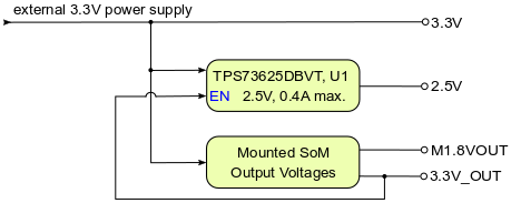
The PL-bank I/O voltages 1.8V, 2.5V and 3.3V will be available after the mounted SoM's 3.3V voltage level has reached stable state on B2B-connector pins JM2-10 and JM2-12, meaning that all on-module voltages have become stable and module is properly powered up.
Following diagram shows the distribution of the external input voltage of nominal 3.3V to the components:
...
Only one supply-source is allowed to configure the base-board supply-voltages, either by jumper, by 0-Ohm-resistor or by connector J6. If a supply-voltage is configured by 0-Ohm-resistor or connector J6, then the corresponding configuration-jumper has to be removed. There aren't 0-Ohm-resistors and supply-voltages by connector J6 allowed if the corresponding base-board supply-voltage is configured by jumper. Vice versa jumpers and 0-Ohm-resistors have to be removed if supplying corresponding base-board supply-voltage by connector J6.
Note: If supplying base-board supply-voltages by connector J6, the module's internal 3.3V voltage-level on pins 9 and 11 of B2B-connector JB2 has to be reached stable state.
| Note |
|---|
Take care of the VCCO voltage ranges of the particular PL IO-banks (HR, HP) of the mounted SoM, otherwise damages may occur to the FPGA. Therefore, refer to the TRM of the mounted SoM to get the specific information of the voltage ranges. It is recommended to set and measure the PL IO-bank supply-voltages before mounting of TE 4 x 5 module to avoid failures and damages to the functionality of the mounted SoM. |
RTC Buffer Voltage Supply Header
The buffer voltage of the SoM's RTC can be supplied through the header J9 (VBAT-pin). Refer to the SoM's TRM for recommended voltage range and absolute maximum ratings.
Push Button
The Carrier Board's push button S2 is connected to the 'RESIN' signal, the function of the button is to trigger a reset of the mounted SoM by driving the reset-signal 'NRST_IN' to ground.
Power and Power-On Sequence
| HTML |
|---|
<!--
If power sequencing and distribution is not so much, you can join both sub sections together
--> |
Power Consumption
The maximum power consumption of the Carrier Board depends mainly on the mounted SoM's FPGA design running on the Zynq device.
Xilinx provide a power estimator excel sheets to calculate power consumption. It's also possible to evaluate the power consumption of the developed design with Vivado. See also Trenz Electronic Wiki FAQ.
...
Table 14: Typical power consumption.
* TBD - To Be Determined soon with reference design setup.
Power supply with minimum current capability of 3A for system startup is recommended.
| Warning |
|---|
| To avoid any damage to the module, check for stabilized on-board voltages and VCCIO's before put voltages on PL I/O-banks and interfaces. All I/Os should be tri-stated during power-on sequence. |
Power Distribution Dependencies
The Carrier Board needs one single power supply voltage with a nominal value of 5V. Following diagram shows the distribution of the input voltage '5VIN' to the on-board components on the mounted SoM:
Figure 5: Board power distribution diagram.
...
| Module Connector (B2B) Designator | VCC / VCCIO | Direction | Pins | Notes | |||
|---|---|---|---|---|---|---|---|
| JB1 | 3.3V | Out | 2, 4, 6, 14, 16 | 3.3V module supply voltage | |||
| VCCIOA | Out | 10, 12 | PL IO-bank VCCIO | ||||
| M1.8VOUT | In | 40 | 1.8V module output voltage | ||||
| VBAT | Out | 80 | RTC buffer voltage | ||||
| JB2 | 1.8V | Out | 2, 4 | 1.8V module supply voltage | |||
| VCCIOB | Out | 6 | PL IO-bank VCCIO | ||||
| VCCIOD | VCCIOC | Out | 8, 10 | PL IO-bank VCCIO | |||
| M33.3VOUT3V_OUT | In | 9, 11 | 3.3V module output voltage | VCCJTAG | In | 9211 | 3.3V JTAG VCCIOmodule output voltage |
| JB3 | USB-VBUS | Out | 56 | USB Host supply voltage |
Table 15: Power pin description of B2B module connector.
| On-board Connector Pin Header Designator | VCC / VCCIO | Direction | Pins | Notes |
|---|---|---|---|---|
| J5 | 3.3V | Out | 6, 45 | 3.3V module supply voltage |
| M3.3VOUT | In | 5, 46 | 3.3V module output voltage | |
| J6 | VCCIOA | Out | B32 | PL IO-bank VCCIO |
| VCCIOC | Out | B1 | PL IO-bank VCCIO | |
| M3.3VOUT | In | C32 | 3.3V module output voltage | |
| 3.3V | Out | C31 | 3.3V module supply voltage | |
| 5VIN | In | A1, A2 | Carrier Board supply power |
...
| Include Page | ||||
|---|---|---|---|---|
|
Variants Currently In Production
...
Operating Temperature
...
Table 21: Board variants.
Technical Specifications
Absolute Maximum Ratings
...
Overview
Content Tools