Page History
...
| B2B Connector | Interfaces | Count of I/O's | Notes |
|---|---|---|---|
| JB1 | User I/O | 42 single ended or 21 differential | - |
| SD IO | 6 | - | |
| MIO | 8 | - | |
| SoM control signals | 1 | 'BOOTMODE' | |
| JB2 | MGT lanes | 8 differential pairs, 4 lanes | - |
| MGT reference input clock | 1 differential pair | ||
| USB2.0 (OTG and device mode) | 4 | - | |
| JB2 | User I/O | 42 single ended 21 differential | -- |
| JTAG | 4 | - | |
| Red user LED | 1 | - | |
| SoM control signals | 1 | 'RESIN' |
Table 1: General overview of PL I/O signals and SoM's interfaces connected to the B2B connectors.
...
The TEBA0841 carrier board is mainly designed for the 4 x 5 SoMs TE0841 and TE0741. This SoMs have GTX-Transceiver units on their FPGA-modules with up to 8 available MGT-lanes. To test this MGT-lanes, 5 RX/TX differential pairs are bridged on-board, hence the transmitted data on this MGT-lanes flows back to their sources in a loop-back circuit without intentional processing or modification.
The MGT lane pins are bridged on-board as fellows, if 4 x 5 SoM TE0741 is mounted on carrier board:
...
The voltage direction of the power rails is from board and on-board connectors' view:
| Module Connector (B2B) Designator | VCC / VCCIO | Direction | Pins | Notes |
|---|---|---|---|---|
| JB1 | 3.3V | Out | 2, 4, 6, 14, 16 | 3.3V module supply voltage |
| VCCIOA | Out | 10, 12 | PL IO-bank VCCIO | |
| M1.8VOUT | In | 40 | 1.8V module output voltage | |
| JB2 |
3.3V_OUT | In | 9, 11 | 3.3V module output voltage | |
| 3.3V |
| Out |
2, 4
| 1, 3, 5, 7 | 3.3V |
| module supply voltage | |||
| VCCIOD | Out | 8, 10 | PL IO-bank VCCIO |
| JB3 | USB-VBUS | Out | 56 | USB Host supply voltage |
Table 15: Power pin description of B2B module connector.
...
| On-board Pin Header Designator | VCC / VCCIO | Direction | Pins | Notes | |||||||
|---|---|---|---|---|---|---|---|---|---|---|---|
| J5J17 | 3.3V | In / Out | 65, 4548 | 3.3V module external supply voltage | |||||||
| VCCIOD | M3.3VOUT | In / Out | 5, 46 | 3.3V module output voltage | 6, 45 | J6 | VCCIOA | Out | B32 | PL IO-bank VCCIO | |
| VCCIOC | Out | B1 | PL IO-bank VCCIO | ||||||||
| , depends on Jumper settings | |||||||||||
| J20 | M3.3VOUT | In | C323.3V | module output voltage3.3V | Out | C31In / Out | 5, 48 | 3.3V | moduleexternal supply voltage | ||
| 5VINVCCIOA | In / Out | A16, A2Carrier Board supply power45 | PL IO-bank VCCIO, depends on Jumper settings |
Table 16: Power Pin description of on-board connector.
...
| Jumper / Header Designator | VCC / VCCIO | Direction | Pins | Notes | ||||
|---|---|---|---|---|---|---|---|---|
| J26 | VCCIOA | OutIn | 2, 4, 6 | - | ||||
| 1M1.8V8VOUT | Out | 1 | - | |||||
| M32.3VOUT5V | Out | 3 | - | |||||
| 3.3V_OUT | Out | 5 | - | |||||
| J27 | VCCIOD | In | 2, 4, 6 | J11 | VCCIOB | Out | 2 | - |
| 1M1.8V8VOUT | Out | 1 | - | |||||
| M32.3VOUT5V | Out | 3 | - | |||||
| 3.3V_OUT | J12 | VCCIOC | Out | 25 | - | |||
| J4 | 13.8V3V | Out | 15 | - | ||||
| M3M1.3VOUT8VOUT | Out | 3 | - |
Table 17: Power Pin description of VCCIO selection jumper pin header.
...
-
...
| 6 | - |
Table 17: Power Pin description of VCCIO selection jumper pin headerTable 18: Main Power jack and pins description.
| Peripheral Socket Designator | VCC / VCCIO | Direction | Pins | Notes | |||||
|---|---|---|---|---|---|---|---|---|---|
| J7 / J8J10 | USB-VBUS | OutIn | 1 | USB2.0 Type A socket / Micro USB2.0 B socket | J4 | M3.3VOUT | Out | 4 | MikroSD Card socket VDDUSB Host supply voltage |
Table 19: Power pin description of peripheral connector.
...
| XMOD Header Designator | VCC / VCCIO | Direction | Pins | Notes | Pins | Notes | |
|---|---|---|---|---|---|---|---|
| JX1 | 3.3V | Out | 5 | connected to 3.3V external supply voltage | |||
| VIO | Out | 6 | |||||
| J3JX1 | 3.3V | -Out | 5 | notconnected | to 3.3V external supply voltage | ||
| 3.3VVIO | Out | 6 | connected to 'VCCJTAG' (pin JB2-92) |
Table 20: Power pin description of XMOD/JTAG Connector.
...
Technical Specifications
Absolute Maximum Ratings
| Parameter | Min | Max | Units |
|---|
| Notes |
|---|
Vin supply voltage |
3.135 | 3.465 |
V
Storage temperature
V | 3.3V supply-voltage ± 5% |
Storage Temperature |
| -55 |
| 105 | °C |
| Molex 74441-0001 Product Specification |
Table 22: Module Board absolute maximum ratings.
Recommended Operating Conditions
Parameter
Reference Document
5VIN
4
75
5
25
V USB2.0 specification concerning 'VBUS' voltage
| Parameter | Min | Max | Units |
|---|
| Notes |
|---|
| Vin supply voltage |
| 3. |
| 135 |
| 3. |
| 465 |
| V | - |
| Operating temperature |
| -40 | +85 | °C | Molex 74441-0001 Product Specification |
Table 23: Module recommended operating conditions.
...
Industrial grade: -40°C to +85°C.
The TE0706 TEBA0841 Carrier Board itself is capable to be operated at industrial grade temperature range.
...
Physical Dimensions
Board size: PCB 100mm × 64.5mm. Notice that the USB type A socket on the left and the Ethernet RJ-45 jacks on the right are hanging slightly over the edge of the PCB making the total width of the longer side approximately 106mm56.47 mm × 75 mm. Notice that some parts the are hanging slightly over the edge of the PCB like the mini USB-jacks and the SFP+ connector, which determine the total physical dimensions of the carrier board. Please download the assembly diagram for exact numbers.
Mating height of the module with standard connectors: 8mm
PCB thickness: ca. 1.65mm
Highest parts part on the PCB are USB type A socket and the Ethernet RJ-45 jacks, approximately 15mmis the SFP+ connector, which has an approximately 11.3 mm overall hight. Please download the step model for exact numbers.
All The dimensions are given in millimetersmm and mil (milli inch).
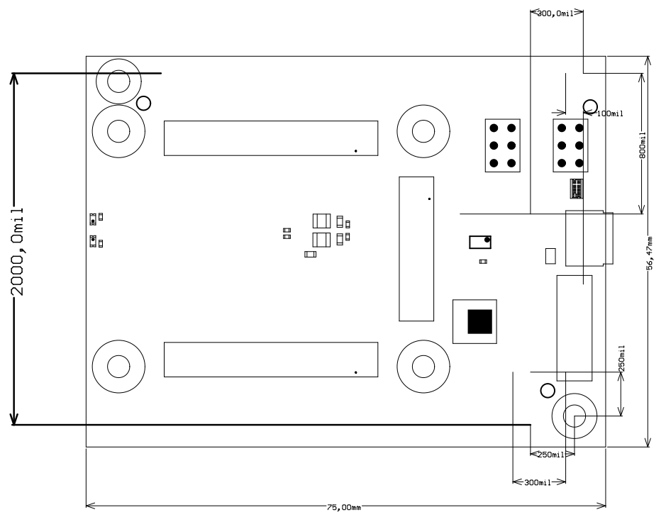
Figure 6: Board physical dimensions drawing.
...
| Date | Revision | Notes | PCN | Documentation Link | 2016-06-28 | 01 |
| - | TE0706-01|
|---|---|---|---|---|---|---|---|---|---|
| -02 | 01 |
|
| - | TEBA0841-01 | - | TE0706-02 |
Table 24: Module hardware revision history.
Hardware revision number can be found on the PCB board together with the module model number separated by the dash.
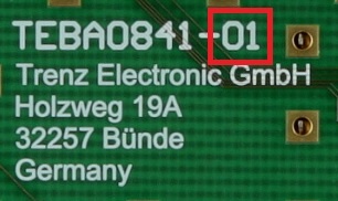
Figure 7: Board hardware revision number.
...
Date | Revision | Contributors | Description | ||||||||||||||||||
|---|---|---|---|---|---|---|---|---|---|---|---|---|---|---|---|---|---|---|---|---|---|
| Ali Naseri |
| 2017-07-06 | v.52 | Ali Naseri, Jan Kumann |
| 2017-01-06 | v.1 | Ali Naseri |
|
Table 25: Document change history.
...
Overview
Content Tools