Page History
...
| On-board Pin Header | Control Signals and Interfaces | Count of I/O's | Notes |
|---|---|---|---|
| J17 | User I/O | 36 single ended or 18 differential | - |
| QSPI interface | 6 | - | |
| J20 | User I/O | 42 single ended or 21 differential | - |
| J3 | JTAG | 4 | - |
| UART | 2 | - | |
| SoM control signals | 2 | 'BOOTMODE', 'PROG_B' | |
| ADC | 1 differential pair | - | |
| MGT reference clock input | 1 differential pair | AC decoupled on-board (100 nF capacitor) | |
| JX1 | JTAG | 4 | - |
| UART | 2 | - | |
| SoM control signals | 2 | 'BOOTMODE', 'PROG_B' | |
| J4 | User I/O | 6 single ended or 3 differential | 3.3V, 3.3V_OUT voltage level available on header |
...
Following diagram shows the distribution of the external input voltage of nominal 3.3V to the components:
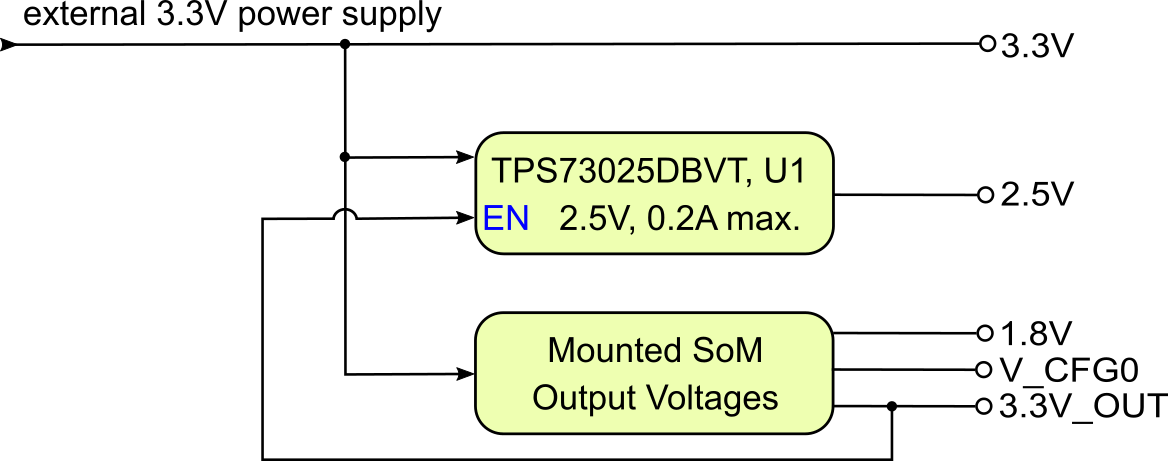
Figure 3: Board power distribution diagram.
...
| Parameter | Min | Max | Units | Notes |
|---|---|---|---|---|
Vin supply voltage | 3.135 | 3.465 | V | 3.3V supply-voltage ± 5% |
Storage Temperature | -40 | 85 | °C | WL-SMCW SMD chip LED data sheet |
Table 20: Board absolute Absolute maximum ratings.
Recommended Operating Conditions
| Parameter | Min | Max | Units | Notes |
|---|---|---|---|---|
| Vin supply voltage | 3.135 | 3.465 | V | - |
| Operating temperature | -40 | +85 | °C | Molex 74441-0001 Product Specification |
Table 21: Module recommended Recommended operating conditions.
Operating Temperature Ranges
...
Physical Dimensions
Board size: PCB 46mm × 75mm. Notice that some parts the are hanging slightly over the edge of the PCB like the the SFP+ connector, which determine the total physical dimensions of the carrier board. Please download the assembly diagram for exact numbers.
Mating height of the module with standard connectors: 8mm
PCB thickness: ca. 1.65mm
Highest part on the PCB is the SFP+ connector, which has an approximately 11.3 mm overall hight. Please download the step model for exact numbers.
...
Overview
Content Tools