Page History
...
The Trenz Electronic TE0723 is a Arduino compatible FPGA module Zynq board with numerous on-board peripherals based on the Xilinx Zynq XC7Z010 SoC.
...
The analog input channels can be selected by the pins 'AMUX_SO', 'AMUX_S1' and 'AMUX_S2', which are connected to the Zynq PL bank 34, pin G12, H12, G11:
| Analog Input Channel | [AMUX_S2:AMUX_S1:AMUX_S0] | Connector pin | Note |
|---|---|---|---|
| AIN0 | 000 | J4-1 | - |
| AIN1 | 001 | J4-2 | - |
| AIN2 | 010 | J4-3 | - |
| AIN3 | 011 | J4-4 | - |
| AIN4 | 100 | J4-5 | - |
| AIN5 | 101 | J4-6 | - |
| AIN6 | 110 | J11-1 | - |
| VIN_SENSE | 111 | - | half divided 5V input supply voltage |
Table 11: Selecting multiplexer analog input channels
Another feature of the analog interface capacities of the XADC units of the Zynq device are the Auxiliary Analog Inputs of the Zynq device's PL bank 35 (see Xilinx document UG480, section 'Auxiliary Analog Inputs'). With 6 pins of female pin header J4 3 analog differential pairs can be created:
| Analog differential Input Pin Pair | Connector pin | Connector pin | Note |
|---|---|---|---|
| IO_L1P_T0_AD0P_35, pin F12 IO_L1N_T0_AD0N_35, pin E13 | J4-3 J4-1 | AIN2 AIN0 | I/O's also usable in digital mode |
IO_L2P_T0_AD8P_35, pin F11 | J4-4 J4-2 | AIN3 AIN1 | I/O's also usable in digital mode |
IO_L3P_T0_DQS_AD1P_35, pin F13 | J4-6 J4-5 | AIN5 AIN4 | I/O's also usable in digital mode |
Table 12: Auxiliary Analog Inputs of the Zynq device
...
Table 13: Reference clock signals.
On-board LEDs
There are three LEDs on-board TE0723:
| LED | Color | Connected to | Description and Notes |
|---|---|---|---|
| D2 | Red | Zynq PS bank 500, pin MIO9 | User LED. |
| D6 | Green | Zynq PL bank 34, pin G14 | User LED. |
| D7 | Green | 3.3V | Indicating 3.3V voltage level. |
Table 14: On-board LEDs
Push Buttons
The TE0723 board is equipped with one push buttons S1:
| Button | Signal Schematic Name | Connected to | Notes |
|---|---|---|---|
| S1 | 'NRST' | Voltage Monitor Circuit, U23 | Triggers system reset. |
Table 15: Push buttons of the module
Power and Power-On Sequence
Power Supply
To power-up a module, power supply with minimum current capability of 1A is recommended.
Power Supply
5V power can be 5V power can be supplied by the external power supply through connector J12 or via USB connection to the host system through USB connector J8 or J9. Minimum current capability of 1A for external power supply is recommended.
Following diagram shows the dependencies of the power supply:
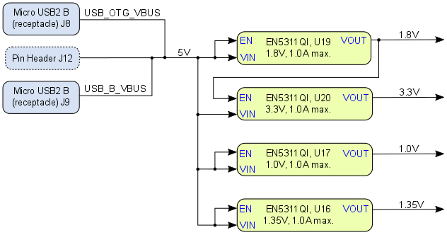
Figure 3: Module power supply dependencies
Power Consumption
Power consumption is to be determined by the user and depends on SoC's FPGA design and connected hardware.
Power-On Sequence
hardware.
| Board Variant | FPGA | Design | Typical Power, 25°C ambient |
|---|---|---|---|
| TE0723-02 | XC7Z010-1CLG225C | Not configured | TBD* |
| TE0723-03M | XC7Z010-1CLG225C | Not configured | TBD* |
| TE0723-03-07S-1C | XC7Z007S-1CLG225C | Not configured | TBD* |
Table 15: Module power consumption
Power-On Sequence
There is no specific power-on sequence, system will power-up automatically when 5V is present either through J8, J9 or J12.
Voltage Monitor Circuit
The voltages 1.0V (core voltage) and 3.3V are monitored by the voltage monitor circuit U23, which generates the POR_B reset signal at power-on. A manual reset is also possible by driving the connector pin J3-3 ('EXT_RST') to GND (leave this pin unconnected or connect to VDD (3.3V) when unused) or press switch button S1, which is assigned to the signal 'NRST'.
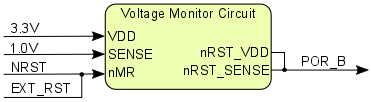
Figure 4: Voltage monitor circuit
Power Rails
The voltage direction of the power rails is directed at on-board connectors' view:
| Header Designator | VCC / VCCIO | Direction | Pins | Notes |
|---|---|---|---|---|
| J6 | VCCIO_33 | In | 2, 4, 6 | - |
| 1.8V | Out | 5 | - | |
| 2.5V | Out | 3 | - | |
| 3.3V | Out | 1 | - | |
| J7 | VCCIO_13 | In | 2, 4, 6 | - |
| 1.8V | Out | 5 | - | |
| 2.5V | OUt | 3 | - | |
| 3.3V | Out | 1 | - |
Table 20: Power Pin description of VCCIO selection jumper pin header.
| Main Power Jack and Pins Designator | VCC / VCCIO | Direction | Pins | Notes |
|---|---|---|---|---|
| J12 | 5VIN | In | 1 | - |
| J9 | 5VIN | In / Out | A1, A2 | also usable as '5VIN' power supply to the Carrier Board as alternative to J12 |
| J2 | VBAT_IN | In | 1 | Attention: Pin 2 connected to ground. VBAT_IN voltage on this pin cause short-circuit. |
Table 21: Main Power jack and pins description.
| Peripheral Socket Designator | VCC / VCCIO | Direction | Pins | Notes |
|---|---|---|---|---|
| J10 / J11 | USB-VBUS | In / Out | 1 | Direction depends on USB2 mode |
| J1 | VIN33 | Out | 4 | MikroSD Card socket VDD |
Table 22: Power pin description of peripheral connector.
Power Rail Name | J3 Pins | J12 Pins | J5 Pins | J6 Pins | J10 Pin | J9 Pins | J8 Pins | Direction | Notes |
|---|---|---|---|---|---|---|---|---|---|
| 3.3V | 5, 6 | 5, 6 | 5, 6 | 12 | 12 | Input | 3.3V power supply voltage | ||
| 5V | |||||||||
| USB_B_VBUS | |||||||||
| USB_OTG_VBUS |
Table 16: Board power rails
Bank Voltages
Bank | Bank I/O Voltage VCCO | Voltage Range |
|---|---|---|
| 0 (config) | 3.3V | fixed |
| 500 (MIO) | 3.3V | fixed |
| 501 (MIO) | 3.3V | fixed |
| 34 (HR) | 3.3V | fixed |
| 35 (HR) | 3.3V | fixed |
There is no specific power-on sequence, system will power-up automatically when 5V is present either through J8, J9 or J12.Table 17: Board bank voltages
Variants Currently in Production
| Module Board Variant | Xilinx Zynq SoC | DDR3L SDRAM | ARM Cores | PL Cells | LUTs | Flip-Flops | Block RAM | DSP Slices |
|---|---|---|---|---|---|---|---|---|
| TE0723-02 | XC7Z010-1CLG225C | 128 MBytes | Dual-core | 28K | 17,6K | 35,2K | 2.1 MBytes | 80 |
| TE0723-03M | XC7Z010-1CLG225C | 512 MBytes | Dual-core | 28K | 17,6K | 35,2K | 2.1 MBytes | 80 |
| TE0723-03-07S-1C | XC7Z007S-1CLG225C | 512 MBytes | Single-core | 23K | 14,4K | 28,8K | 1.8 MBytes | 66 |
Table 1018: Module Board variants.
Technical Specifications
Absolute Maximum Ratings
Parameter | Min | Max | Units | Reference Document |
|---|---|---|---|---|
VIN supply voltage | -0.5 | 3.6 | V | Xilinx datasheet DS187. |
Storage temperature | -40 | +85 | °C |
Table 1119: TE0723 module Board absolute maximum ratings.
...
| Parameter | Min | Max | Units | Reference Document |
|---|---|---|---|---|
| Supply voltage | 1.14 | 3.465 | V | Xilinx datasheet DS187. |
Table 1220: TE0723 module Board recommended operating conditions.
| Note |
|---|
| Please check Xilinx datasheet DS187 for complete list of absolute maximum and recommended operating ratings for the Zynq-7 deviceAssembly variants for higher storage temperature range are available on request. |
Physical Dimensions
Module size: 68.58 mm × 53.34 mm. Please download the assembly diagram for exact numbers.
PCB thickness: 1.6 mm.
Highest part on PCB: approx. 4 mm. Please download the step model for exact numbers.
Please note that two different units are used on the figures below, SI system millimeters (mm) and imperial system thousandths of an inch(mil). To convert mils to millimeters and vice versa use formula 100mil's = 2,54mm.
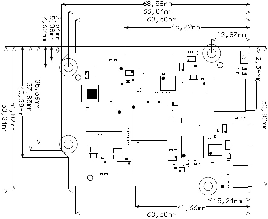
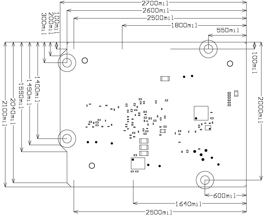
Figure 3: TE0723 module physical dimensions.
Operating Temperature Ranges
Commercial grade: 0°C to +70°C.
Industrial grade: -40°C to +85°C.
54mm.
Figure 5: Board physical dimensionsOperating temperature range depends also on customer design and cooling solution. Please contact us for options.
Revision History
Hardware Revision History
| Date | Revision | Notes | PCN | Documentation Link | |
|---|---|---|---|---|---|
| 2016-07-15 | 03 | Refer to Changes list in Schematic for further details in changes to REV02 | -Click to see PCN. | TE0723-03 | |
2015-11-06 | 02 | Second Production Release | - | TE0723-02 | |
| - | 01 | First Production Release | - | - |
Table 1321: TE0723 Board hardware revision history.
Hardware revision number is printed on the PCB board together with the module model number separated by the dash.
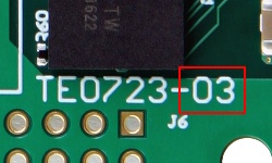
Figure 6: TE0723 board hardware revision number
Document Change History
Date | Revision | Contributors | Description | ||||||||
|---|---|---|---|---|---|---|---|---|---|---|---|
| Ali Naseri, | Initial document.
|
Table 1422: Document change history.
...
Overview
Content Tools