Page History
...
| FPGA SoC Signal | Pin | Pmod Signal | Pmod Pin |
|---|---|---|---|
| MSIO71PB7 | U2-F3 | PB-01 | P1-1 |
| MSIO71NB7 | U2-F4 | PB-02 | P1-2 |
| MSIO68NB7 | U2-E3 | PB-03 | P1-3 |
| MSIO80NB7 | U2-H4 | PB-04 | P1-4 |
| MSIO75PB7 | U2-G4 | PB-05 | P1-7 |
| MSIO75NB7 | U2-F5 | PB-06 | P1-8 |
| MSIO67NB7 | U2-E5 | PB-07 | P1-9 |
| MSIO78NB7 | U2-G3 | PB-08 | P1-10 |
| MSIO79PB7 | U2-G1 | PC-01 | P2-1 |
| MSIO79NB7 | U2-F1 | PC-02 | P2-2 |
| MSIO70NB7 | U2-E2 | PC-03 | P2-3 |
| MSIO64PB7 | U2-C1 | PC-04 | P2-4 |
| MSIO78PB7 | U2-G2 | PC-05 | P2-7 |
| MSIO70PB7 | U2-E1 | PC-06 | P2-8 |
| MSIO68PB7 | U2-D2 | PC-07 | P2-9 |
| MSIO64NB7 | U2-C2 | PC-08 | P2-10 |
| MSIO117NB4 | U2-Y16 | PA-01 | P3-1 |
| MSIO117PB4 | U2-Y15 | PA-02 | P3-2 |
| MSIO112PB4 | U2-W13 | PA-03 | P3-3 |
| MSIO110PB4 | U2-V12 | PA-04 | P3-4 |
| MSIO118PB4 | U2-W15 | PA-05 | P3-7 |
| MSIO112NB4 | U2-W14 | PA-06 | P3-8 |
| MSIO105NB4 | U2-Y13 | PA-07 | P3-9 |
| MSIO104PB4 | U2-V11 | PA-08 | P3-10 |
| MSIO4PB2 | U2-P20 | PD-01 | P4-1 |
| MSIO3NB2 | U2-R20 | PD-02 | P4-2 |
| MSIO2NB2 | U2-T19 | PD-03 | P4-3 |
| MSIO0PB2 | U2-V20 | PD-04 | P4-4 |
| MSIO6NB2 | U2-P19 | PD-05 | P4-7 |
| MSIO3PB2 | U2-T20 | PD-06 | P4-8 |
| MSIO1NB2 | U2-U19 | PD-07 | P4-9 |
| MSIO0NB2 | U2-V19 | PD-08 | P4-10 |
Table 3: Overview of Pmod signals connected to the SoC.
JTAG Interface
JTAG access to the SoC components is provided through the micro usb connector via the FTDI usb to UART bridge. Depending on the jumper J6 the JTAGSEL signal SW3 switches the JTAG interface to either the FPGA fabric TAP (OPEN, high) or the Cortex-M3 JTAG debug interface (CLOSED, low). JTAG signals are powered by 3.3V.
FTDI signal | pin | JTAG Signal | Microsemi SmartFusion2 SoC pin |
|---|---|---|---|
| ADBUS0 | U3-12 | TCK | U2-W19 |
| ADBUS1 | U3-13 | TDI | U2-V16 |
| ADBUS2 | U3-14 | TDO | U2-Y20 |
| ADBUS3 | U3-15 | TMS | U2-V17 |
Table 54: JTAG interface signals.
SD Card Interface
...
| FPGA / SoC Pin | Connected To | Signal Name | Notes |
|---|---|---|---|
| U2-H16 | J3-9 | SD_CD | Card detect switch |
| U2-N15 | J3-7 | SD_D0 | |
| U2-G18 | J3-8 | SD_D1 | |
| U2-R16 | J3-1 | SD_D2 | |
| U2-R17 | J3-2 | SD_D3 | |
| U2-R15 | J3-3 | SD_CMD | |
| U2-P15 | J3-5 | SD_CLK |
Table 65: SD Card interface signals and connections.
...
| PHY Pin | Signal | Microsemi SmartFusion2 SoC signal | Pin | Notes |
|---|---|---|---|---|
| U1-25 | ETH_TXCK | MSIOD84PB6 | U2-K7 | |
| U1-23 | ETH_TXCTL | MSIOD87NB6 | U2-K3 | |
| U1-26 | ETH_TXD0 | MSIOD93PB6 | U2-L1 | |
| U1-28 | ETH_TXD1 | MSIOD97NB6 | U2-M2 | |
| U1-29 | ETH_TXD2 | MSIOD97PB6 | U2-M1 | |
| U1-30 | ETH_TXD3 | MSIOD95PB6 | U2-M3 | |
| U1-22 | ETH_RRXCK | MSIOD84PB6 | U2-J2 | |
| U1-21 | ETH_RRXCTL | MSIOD93NB6 | U2-K1 | |
| U1-20 | ETH_RRXD0 | MSIOD86PB6 | U2-K5 | |
U1-18 | ETH_RRXD1 | MSIOD82PB6 | U2-H1 | |
| U1-17 | ETH_RRXD2 | MSIOD82NB6 | U2-H2 | |
| U1-16 | ETH_RRXD3 | MSIOD83PB6 | U2-J4 | |
| U1-31 | ETH_MDC | MSIOD99PB6 | U2-N1 | |
| U1-33 | ETH_MDIO | MSIOD99NB6 | U2-N2 | |
| U1-34 | ETH_MDINT | MSIOD98PB6 | U2-N4 | |
| U1-35 | ETH_RST | MSIO114PB4 | U2-R13 | |
| U1-36 | PHY_RCLKOUT | MSIO102NB4/CCC_NE1_CLKIO | U2-W10 | |
| U1-39 | PHY_LED0 | MSIO104NB4 | U2-U11 | |
| U1-38 | PHY_LED1 | MSIO116PB4 | U2_T14 |
Table 76: Ethernet PHY signals and connections.
...
| I2C Device | I2C Address | Notes |
|---|---|---|
| Header J8 | 0x50 | Device detection/identification. |
Table 87: I2C slave device addresses.
...
| Clock Source | Schematic Name | Frequency | Clock Destination |
|---|---|---|---|
| Crystal CX3225CA25000D0HSSCC | Y1 | 25.000 MHz1 | SmartFusion2 SoC U2 Main XTAL |
| Crystal ECX-31B | Y2 | 32.768 KHz | SmartFusion2 SoC U2 AUX XTAL |
| SiTime SiT8008AI oscillator | U11 | 25.000000 MHz | Gb Ethernet Copper PHY U1A |
| SiTime SiT8008AI oscillator | U14 | 25.000000 MHz | SmartFusion2 SoC U2-Y12 Bank 4 |
Table 98: Reference clock signals.
...
On-board LEDs
| LED | Color | Connected to | SoC FPGA Signal | Description and Notes |
|---|---|---|---|---|
| D1 | Red | U2-G16 Bank 1 | MSIO21PB1 | |
| D2 | Green | U2-G17 Bank 1 | MSIO21NB1 | |
| D3 | RGB | U2-H5 Bank 7, U2-F6 Bank 7, U2-H6 Bank 7 | MSIO80PB7, MSIO67PB7, MSIO81NB7 | |
| J2 | Green, Yellow | U2-Y10 Bank 4, U2-U12 Bank 4 | MSIO102PB4, MSIO110NB4 | Ethernet: LED1A, LED1B |
| J2 | Green, Yellow | U2-V14 Bank 4, U2-U14 Bank 4 | MSIO115PB4, MSIO115PB4 | Ethernet: LED2A, LED2B |
Table 109: On-board LEDs.
On-board Buttons
| Button | Connected to | SoC FPGA Signal |
|---|---|---|
| S4 | U2-E17 Bank 1 | MSIO24PB1 |
| S5 | U2-E16 Bank 1 | MSIO24NB1 |
Table 10: On-board Buttons.
...
| Module Variant | FPGA / SoC | Operating Temperature | Temperature Range |
|---|---|---|---|
| TEM0002-01 | M2S010 | 0°C to +70°C | commercial |
Table 14: Module variants.
Technical Specifications
...
Parameter | Min | Max | Units | Reference Document |
|---|---|---|---|---|
VIN supply voltage | -0.3 | 6.0 | V | - |
Storage temperature1 | -25 | 70 | °C | - |
Table 15: Module absolute maximum ratings.
...
| Parameter | Min | Max | Units | Reference Document |
|---|---|---|---|---|
| VIN supply voltage | 2.4 | 5.5 | V | - |
| Operating temperature1 | 0 | 70 | °C | - |
Table 16: Module recommended operating conditions.
...
All dimensions are given in millimeters.
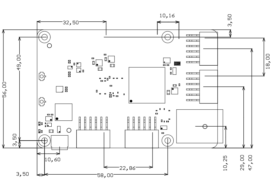
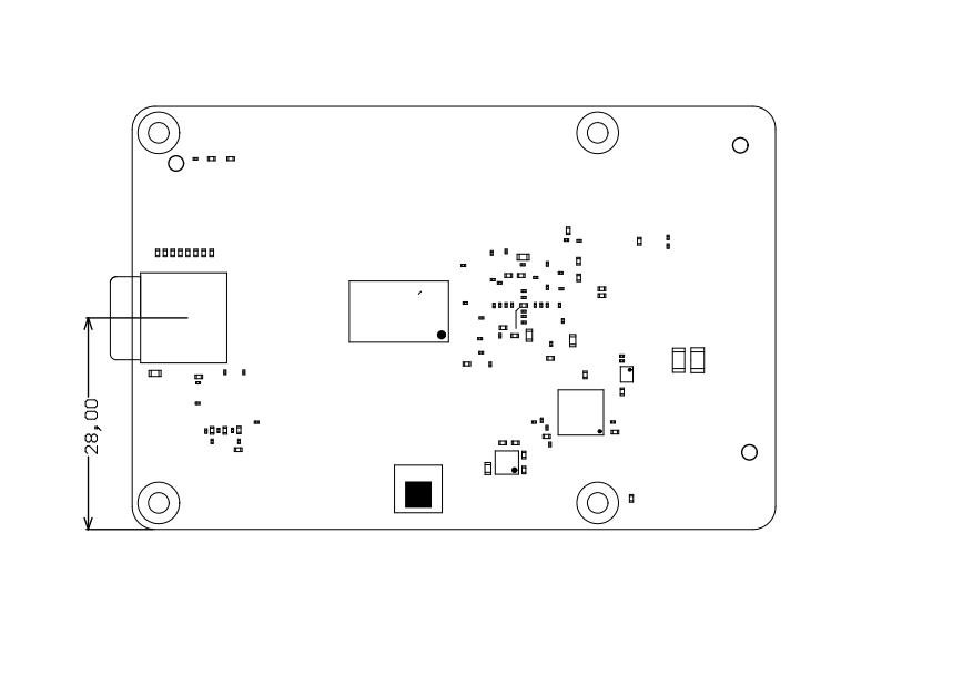
Figure 4: Module physical dimensions drawing.
...
| Date | Revision | Notes | PCN | Documentation Link |
|---|---|---|---|---|
| - | 01 | Prototypes |
Table 17: Module hardware revision history.
...
draw.io Diagram border false viewerToolbar true fitWindow false diagramName Pic_REV_number simpleViewer true width 200 links auto tbstyle top lbox true diagramWidth 1571 revision 3
Figure 5: Module hardware revision number.
...
Date | Revision | Contributors | Description | ||||||||
|---|---|---|---|---|---|---|---|---|---|---|---|
|
| ||||||||||
all | Jan Kumann, John Hartfiel |
Table 18: Document change history.
...
Overview
Content Tools