Page History
...
| Scroll Title | ||
|---|---|---|
| ||
|
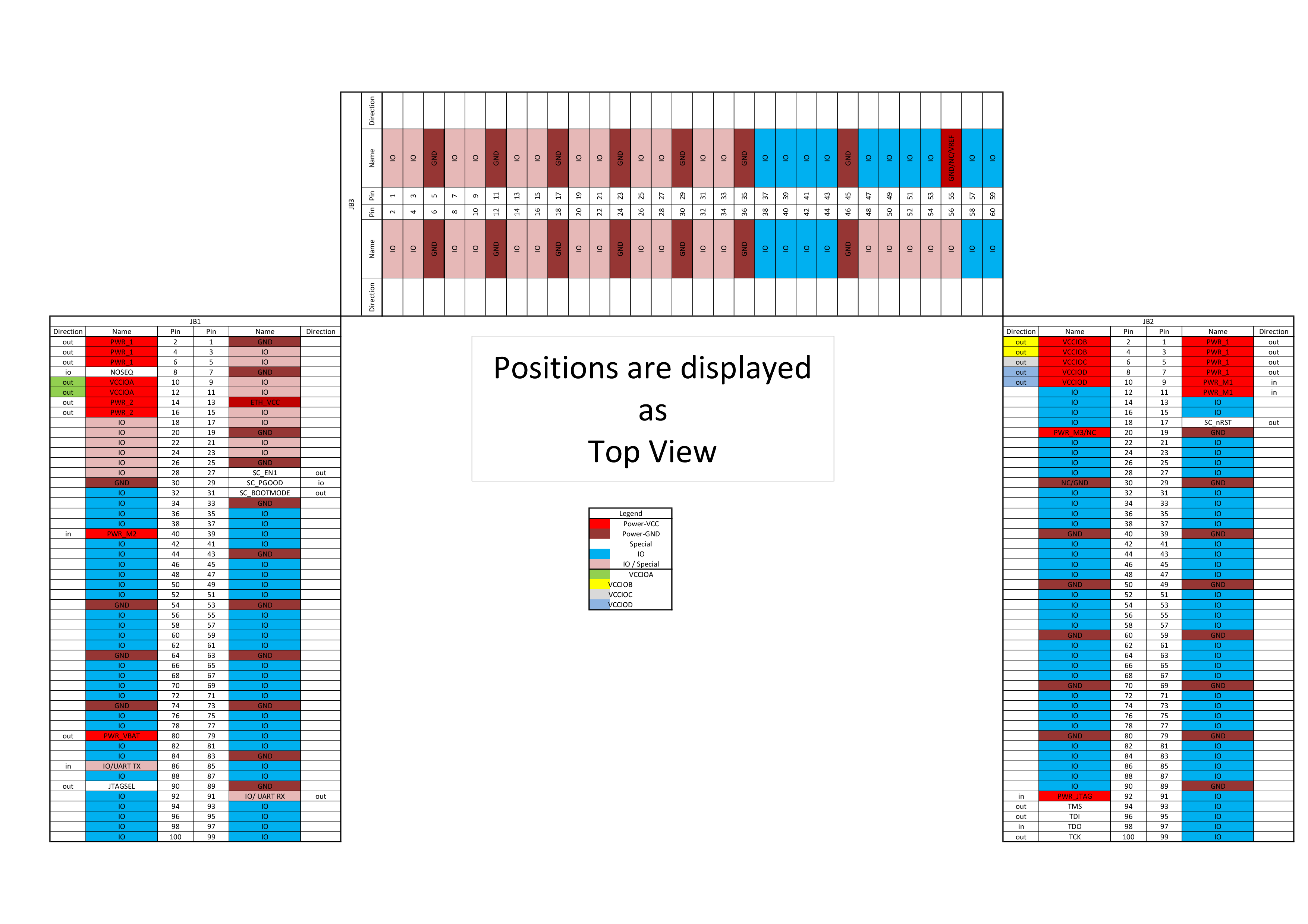
4x5 Module Controller IOs
| Name | Module B2B Pin | Carrier B2B Pin | Description | Recommendation |
|---|---|---|---|---|
| JTAGSEL | JM1-89 | JB1-90 | JTAG Chain multiplexer. Low FPGA, High CPLD. For module with CPLD only. | Connect Pulldown on carrier. |
| SC_EN1 | JM1-28 | JB1-27 | Module power . Set high to enable module power. Note: Power management depends on module. Sometimes this is a only used as Power ON Reset like SC_nRST | Connect Pullup on carrier. DIP switch possible |
| SC_NOSEQ | JM1-7 | JB1-8 | Module Power management. Set high to disable CPLD power management. Note: Power management depends on module and not all modules support extended power management with CPLD. | Connect Pullup on carrier. DIP switch possible. |
| SC_PGOOD | JM1-30 | JB1-29 | Power Good signal. Is Low, if SC_EN1 is set to zero or if power is not ready, otherwise high impedance output. Note: Power management depends on module. | Connect Pullup on carrier. This signal or one of the module output voltages can be used to activate Bank power from external regulator via power switch. |
| SC_BOOTMODE | JM1-32 | JB1-31 | Boot Mode selection Pin for Zynq module only. Default low for primary SD boot and high for primary QSPI boot. Note: Depends also on module CPLD firmware | Connect Pullup on carrier. DIP switch possible. |
| SC_nRST | JM2-18 | JB1-17 | Low active module reset. Pin force Power one reset on FPGA/SoC. Note: Depending from module CPLD or voltage supervisor is used. | Connect Pullup on carrier. DIP switch possible. |
Remove 4x5 module
| Widget Connector | ||
|---|---|---|
|
...
Overview
Content Tools