Page History
...
| Scroll Only (inline) |
|---|
Refer to https://wiki.trenz-electronic.de/display/PD/TE0720+TRM for online version of this manual and additional technical documentation of the product. |
The Trenz Electronic TE0720 is an industrial-grade SoM (System on Module) based on Xilinx Zynq-7000 SoC (XC7Z020 or XC7Z014S) with up to 1 GB of DDR3/L SDRAM, 32MB of SPI flash memory, Gigabit Ethernet PHY transceiver, a USB PHY transceiver and powerful switching-mode power supplies for all on-board voltages. A large number of configurable I/Os is provided via rugged high-speed stacking strips. See also Variants Currently in Production section.
...
- Xilinx XC7Z SoC (XC7Z020 or XC7Z014S)
- Processing system (PS):
- XC7Z020: Dual-core ARM Cortex-A9 MPCore™ with CoreSight™
- XC7Z014S: Single-core ARM Cortex-A9 MPCore™ with CoreSight™
- L1 cache: 32 KByte instruction, 32 KByte data per processor
- L2 cache: Unified 512 KByte
- Programmable logic (PL): Artix-7 FPGA
- Programmable logic cells: 85K (XC7Z020), 65K (XC7Z014S)
- Block RAM: 4.9 MByte (XC7Z020), 3.8 MByte (XC7Z014S)
- DSP slices: 220 (XC7Z020), 170 (XC7Z014S)
- Peak DSP performance: 276 GMACs (XC7Z020), 187 GMACs (XC7Z014S)
- 2x 12 bit, MSPS ADCs with up to 17 differential inputs
- Processing system (PS):
- 54 multiuse I/O (MIO) pins
- 152 High-Range (HR) I/O pins (SelectIO interfaces)
- System Controller CPLD (Lattice LCMXO2-1200HC)
- Up to 1 GByte DDR3/L SDRAM memory (2 x 256 Mbit x 16, 32-bit wide data bus).
- 32 MByte Quad SPI Flash memory
- Gigabit Ethernet transceiver PHY (Marvell 88E1512)
- MAC address serial EEPROM with EUI-48™ node identity (11AA02E48)
- Highly integrated full-featured hi-speed USB 2.0 ULPI transceiver (Microchip USB3320C-EZK)
- 3-axis accelerometer and 3-axis magnetometer (ST Microelectronics LSM303DTR) (Optional!)
- Real time clock with embedded crystal (Intersil ISL12020M): ±5ppm accuracy
- Atmel CryptoAuthentication element (Atmel ATSHA204A)
- Up to 32 GByte eMMC, usually 4 GByte, depends on module variant and assembly option
- User LED 1 (Green), user LED 2 (Red), user LED 3 - FPGA DONE (Green)
- On-board high-efficiency DC-DC converters for all voltages used
- Trenz 4 x 5 module socket connectors (3 x Samtec LSHM series connectors)
- Evenly spread supply pins for good signal integrity
- Rugged for shock and high vibration
...
Table 2: General PL I/O to B2B connectors information.
PS MIO bank 500 and 501 signal connections to B2B JM1 connector, 14 PS MIOs total.
| MIO | B2B Pin | Bank | Voltage | Notes | |
|---|---|---|---|---|---|
| 0 | JM1-87 | 500 | 3.3V | ||
| 9 | JM1-91 | 500 | 3.3V | ||
| 10 | JM1-95 | 500 | 3.3V | ||
| 11 | JM1-93 | 500 | 3.3V | ||
| 12 | JM1-99 | 500 | 3.3V | ||
| 13 | JM1-97 | 500 | 3.3V | ||
| 14 | JM1-92 | 500 | 3.3V | Also wired to U19-M4 | |
| 15 | JM1-85 | 500 | 3.3V | Also wired to U19-N4 | |
| 40 | JM1-27 | 501 | 1.8V | Zynq SoC SD0 | |
| 41 | JM1-25 | 501 | 1.8V | Zynq SoC SD0 | |
| 42 | JM1-23 | 501 | 1.8V | Zynq SoC SD0 | |
| 43 | JM1-21 | 501 | 1.8V | Zynq SoC SD0 | |
| 44 | JM1-19 | 501 | 1.8V | Zynq SoC SD0 | |
| 45 | JM1-17 | 501 | 1.8V | Zynq SoC SD0 |
...
Table 4: JTAG pins connection.
| Note |
|---|
| JTAGMODE pin 89 in B2B connector JM1 is used to switch access between devices, low selects Zynq SoC, high selects System Controller CPLD. |
...
Ethernet PHY to B2B connections
| PHY Signal | B2B Pin | PHY Signal | B2B Pin | ||
|---|---|---|---|---|---|
| SOUT_N | JM3-1 | PHY_MDI1_P | JM1-10 | ||
| SOUT_P | JM3-3 | PHY_MDI1_N | JM1-12 | ||
| SIN_N | JM3-2 | PHY_MDI2_P | JM1-16 | ||
| SIN_P | JM3-4 | PHY_MDI2_N | JM1-18 | ||
| PHY_MDI0_P | JM1-4 | PHY_MDI3_P | JM1-22 | ||
| PHY_MDI0_N | JM1-6 | PHY_MDI3_N | JM1-24 |
Table 8: Ethernet PHY to B2B connections.
Ethernet PHY to Zynq SoC PS MIO ETH0 connections
| PHY Signal | SoC MIO | PHY Signal | SoC MIO | ||
|---|---|---|---|---|---|
| ETH-TXCK | 16 | ETH-RXCK | 22 | ||
| ETH-TXD0 | 17 | ETH-RXD0 | 23 | ||
| ETH-TXD1 | 18 | ETH-RXD1 | 24 | ||
| ETH-TXD2 | 19 | ETH-RXD2 | 25 | ||
| ETH-TXD3 | 20 | ETH-RXD3 | 26 | ||
| ETH-TXCTL | 21 | ETH-RXCTL | 27 | ||
| ETH-MDC | 52 | ETH-MDIO | 53 |
Table 9: Ethernet PHY to Zynq SoC connections.
...
| USB PHY Pin | SC CPLD Pin | B2B Name | Notes | |
|---|---|---|---|---|
| REFSEL0..2 | - | - | Reference clock frequency select, all set to GND = 52.000000 MHz. | |
| RESETB | B14, bank 1 | - | Active low reset. | |
| CLKOUT | - | - | ULPI output clock connected to Zynq PS MIO36. | |
| DP, DM | OTG-D_P, OTG-D_N | USB data lines. | ||
| CPEN | VBUS_V_EN | External USB power switch active high enable signal. | ||
| VBUS | - | USB-VBUS | Connect to USB VBUS via a series of resistors, see reference schematic. | |
| ID | - | OTG-ID | For A-device connect to the ground, for B-device leave floating. | |
| SPK_L | M5, bank 2 | - | In USB audio mode a switch connects the DM pin to the SPK_L. | |
| SPK_R | M8, bank 2 | - | In USB audio mode a switch connects the DP pin to the SPK_R. |
...
| LED | Color | Connected to | Description and Notes | |
|---|---|---|---|---|
| D2 | Green | LED1 | Controlled by System Controller CPLD firmware. | |
| D4 | Green | DONE | ||
| D5 | Red | LED2 | Controlled by System Controller CPLD firmware. |
...
| Note |
|---|
Current rating of Samtec Razor Beam™ LSHM B2B connectors is 2.0A per pin (2 adjacent pins powered). |
...
| Page break |
|---|
Power-On Sequence
...
NOSEQ input signal from the carrier board can be used to control output of the two DC-DC converters U1 and U3. It works in conjunction with the System Controller CPLD firmware controlled ON_1V0 and ON_1V8 input signals of the U21 and U25 gate ICs.
|
|
| If NOSEQ input signal from the carrier board is low (logical 0), signals ON_1V0 and ON_1V8 can be driven by System Controller CPLD to control outputs of the U1 and U3 DC-DC converters. | If NOSEQ input signal from the carrier board is high (logical 1), state of the ON_1V0 and ON_1V8 signals is irrelevant and DC-DC converters U1 and U3 outputs are always enabled. |
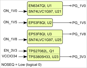
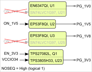
Figure 4: Power sequencing.
| Note |
|---|
Initial state of the ON_1V0 and ON_1V8 signals and therefore also functionality of the NOSEQ signal depend on the System Controller CPLD firmware. |
...
Bank | Schematic Name | Voltage | Notes | |
|---|---|---|---|---|
| 500 | 3.3V, VCCO_MIO0_500 | 3.3V | ||
| 501 | 1.8V, VCCO_MIO1_501 | 1.8V | ||
| 502 | 1.5V, VCCO_DDR_502 | 1.5V | ||
| 0 Config | 3.3V | 3.3V | ||
| 13 HR | VCCO13 | 1.2V to 3.3V | Supplied by the carrier board. | |
| 33 HR | VCCIO33 | 1.2V to 3.3V | Supplied by the carrier board. | |
| 34 HR | VCCIO34 | 1.2V to 3.3V | Supplied by the carrier board. | |
| 35 HR | VCCIO35 | 1.2V to 3.3V | Supplied by the carrier board. |
...
Table 22: Module absolute maximum ratings.
| Note |
|---|
| Assembly variants for higher storage temperature range are available on request. |
...
Table 24: Hardware revision history table.
...
Overview
Content Tools