Page History
...
| Scroll Only (inline) |
|---|
Refer to https://wiki.trenz-electronic.de/display/PD/TE0782+TRM for online version of this manual and the rest of available documentation. |
The Trenz Electronic TE0782 is a high-performance, industrial-grade SoM (System on Module) with industrial temperature range based on Xilinx Zynq-7000 SoC (XC7Z035, XC7Z045 or XC7Z100).
...
Block Diagram
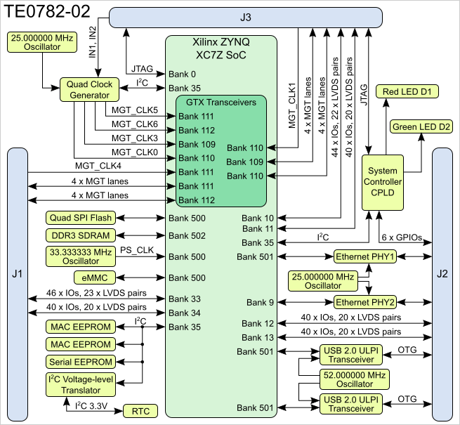
Main Components
- Xilinx Zynq XC7Z SoC (XCZ035, XC7Z045 or XC7Z100), U1
- Lattice Semiconductor MachXO2 1200HC System Controller CPLD, U14
- Intelligent Memory 4Gbit DDR3L-1600 SDRAM, U19
- Intelligent Memory 4Gbit DDR3L-1600 SDRAM, U10
- Spansion 32 MByte QSPI Flash memory, U38
- SI5338A PLL programmable clock generator, U2
- TI low-dropout linear regulator @1.5V, U23
- Microchip USB3320C USB PHY transceiver, U8
- Microchip USB3320C USB PHY transceiver, U4
Intersil ISL12020MIRZ Real Time Clock, U17
- LT quad 4A PowerSoC DC-DC converter (1.0V), U13
LT quad 4A PowerSoC DC-DC converter (3.3V, 1,8V, 1.2V_MGT, 1.0V_MGT), U16
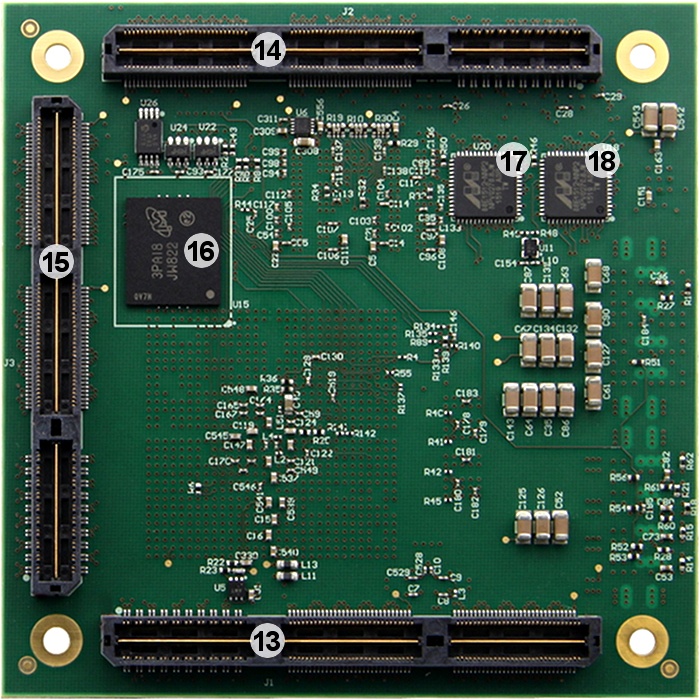
- Samtec ASP-122952-01 160-pin stacking strip (2 rows a 80 positions), J1
- Samtec ASP-122952-01 160-pin stacking strip (2 rows a 80 positions), J2
- Samtec ASP-122952-01 160-pin stacking strip (2 rows a 80 positions), J3
Micron Technology 4 GByte eMMC, U15
- Marvell Alaska 88E1512 Gigabit Ethernet PHY, 20
- Marvell Alaska 88E1512 Gigabit Ethernet PHY, U18
...
| Storage device name | Content | Notes | |
|---|---|---|---|
| 24LC128-I/ST | not programmed | User content | |
24AA025E48 EEPROM's | User content not programmed | Valid MAC Address from manufacturer | |
| eMMC Flash-Memory | Empty, not programmed | Except serial number programmed by flash vendor | |
SPI Flash OTP Area | Empty, not programmed | Except serial number programmed by flash vendor | |
SPI Flash Quad Enable bit | Programmed | ||
SPI Flash main array | demo design | ||
| HyperFlash RAM | not programmed | ||
eFUSE USER | Not programmed | ||
eFUSE Security | Not programmed |
Signals, Interfaces and Pins
...
| Bank | Type | VCCIO Max | Connector | IO count | Differential | IO Voltage | Notes | |
|---|---|---|---|---|---|---|---|---|
| 10 | HR | 3.3V | J3 | 44 | 22 | user | ||
| 11 | HR | 3.3V | J3 | 40 | 20 | user | ||
| 12 | HR | 3.3V | J2 | 40 | 20 | user | ||
| 13 | HR | 3.3V | J2 | 40 | 20 | user | ||
| 33 | HP | 1.8V | J1 | 48 | 23 | user | ||
| 34 | HP | 1.8V | J1 | 42 | 20 | user |
For detailed information about the pin out, please refer to the Master pin-out table.
...
| Name | Connection | Note | |
|---|---|---|---|
| CLPD_GPIO7 | B2B | Function defined by CPLD Firmware (legacy name was BOOTMODE) | |
| CLPD_GPIO6 | B2B | Function defined by CPLD Firmware (legacy name was CONFIGX) | |
| JTAGENB | B2B | Logic high enables CPLD JTAG pins, when low CPLD JTAG access is disabled | |
| nRST_IN | B2B | Active low System-reset input (old name RESIN) | |
| CLPD_GPIO0 | B2B | Function defined by CPLD Firmware | |
| CLPD_GPIO1 | B2B | Function defined by CPLD Firmware | |
| CLPD_GPIO2 | B2B | Function defined by CPLD Firmware | |
| CLPD_GPIO3 | B2B | Function defined by CPLD Firmware | |
| CLPD_GPIO4 | B2B | Function defined by CPLD Firmware | |
| CLPD_GPIO5 | B2B | Function defined by CPLD Firmware | |
| CPLD_IO | PL |
Some of the functions of the SoM are controlled by the System Controller CPLD and it's firmware. User can change this by using(creating) different firmware for the System Controller CPLD.
...
| Clock | Frequency | IC | Zynq PS / PL | Notes | ||
|---|---|---|---|---|---|---|
| PS CLK | 33.333333 MHz | U61 | PS CLK | PS subsystem main clock | ||
| ETH PHY reference | 25.000000 MHz | U11 | - | |||
| USB PHY reference | 52.000000 MHz | U7 | - | |||
PLL reference | 25.000000 MHz | U3 | - | |||
GT REFCLK1 | - | B2B connector | Bank 110, pin AC7/AC8 | Supplied from baseboard. | ||
GT REFCLK4 | - | B2B connector | Bank 111, pin U7/U8 | Supplied from baseboard. | ||
| Si5338 CLK0 | U2 | Bank 110, pin AA8/AA7 | ||||
| Si5338 CLK1 | U2 | Bank 109, pin AF10/AF9 | ||||
| Si5338 CLK2 | U2 | Bank 111, pin W8/W7 | ||||
| Si5338 CLK3 | U2 | Bank 112, pin N8/N7 |
Default MIO Mapping
| MIO | Configured as | B2B | Notes |
|---|---|---|---|
| 0 | USB Reset | - | CPLD used as level translator |
| 1 | QSPI0 | - | SPI Flash-CS |
| 2 | QSPI0 | - | SPI Flash-DQ0 |
| 3 | QSPI0 | - | SPI Flash-DQ1 |
| 4 | QSPI0 | - | SPI Flash-DQ2 |
| 5 | QSPI0 | - | SPI Flash-DQ3 |
| 6 | QSPI0 | - | SPI Flash-SCK |
| 7 | Ethernet Reset | - | CPLD used level translator |
| 8 | UART TX | JC3:129 | output, muxed to B2B by the SC CPLD |
| 9 | UART RX | JC3:135 | input, muxed to B2B by the SC CPLD |
| 10 | SDIO1 D0 | - | - |
| 11 | SDIO1 CMD | - | - |
| 12 | SDIO1 CLK | - | - |
| 13 | SDIO1 D1 | - | - |
| 14 | SDIO1 D2 | - | - |
| 15 | SDIO1 D3 | - | - |
| 16..27 | ETH0 | - | Ethernet RGMII PHY |
| 28..39 | USB0 | - | USB0 ULPI PHY |
| 40...51 | USB1 | - | USB1 ULPI PHY |
| 52 | ETH0 MDC | - | - |
| 53 | ETH0 MDIO | - | - |
...
| PHY PIN | ZYNQ PS / PL | System Controller CPLD | Notes | |
|---|---|---|---|---|
| MDC/MDIO | MIO52, MIO53 | - | - | |
| LED0 | BANK35, Pin B12 | - | - | |
| LED1 | BANK35, Pin C12 | - | - | |
| Interrupt | BANK35, Pin A15 | - | - | |
| CONFIG | BANK35, Pin F14 | - | - | |
| RESETn | - | Pin 53 | ETH1_RESET33 (MIO7) -> CPLD -> ETH1_RESET | |
| RGMII | MIO16..MIO27 | - | ||
| MDI | - | - | on B2B J2 connector |
...
| Device | IC | Designator | I2C-Address | Notes |
|---|---|---|---|---|
| EEPROM | 24LC128-I/ST | U26 | 0x53 | user data, parameter |
| EEPROM | 24AA025E48T-I/OT | U22 | 0x50 | MAC address EEPROM |
| EEPROM | 24AA025E48T-I/OT | U24 | 0x51 | MAC address EEPROM |
| RTC | ISL12020MIRZ | U17 | 0x6F | Temperature compensated real time clock |
| Battery backed RAM | ISL12020MIRZ | U17 | 0x57 | Integrated in RTC |
| PLL | SI5338A-B-GMR | U2 | 0x70 | |
| CPLD | LCMXO2-1200HC-4TG100I | U14 | user | - |
...
| Peripheral | IC | Designator | Zynq PS / PL | MIO | Notes | ||
|---|---|---|---|---|---|---|---|
| QSPI Flash | S25FL256SAGBHI20 | U38 | PS QSPI0 | MIO1...MIO6 | - | ||
| ETH0 10/100/1000 Mbps PHY | 88E1512-A0-NNP2I000 | U18 | PS ETH0 | MIO16...MIO27, MIO52, MIO53 | - | ||
| ETH0 10/100/1000 Mbps PHY Reset | PS GPIO | MIO7 | ETH1_RESET33 (MIO7) -> CPLD -> ETH1_RESET | ||||
| ETH1 10/100/1000 Mbps PHY | 88E1512-A0-NNP2I000 | U20 | BANK9, BANK35 | - | PHY can be used with soft Ethernet MAC IP also | ||
| ETH1 10/100/1000 Mbps PHY Reset | BANK35, Pin B15 | - | - | ||||
| USB0 | USB3320C-EZK | U4 | PS USB0 | MIO28...MIO39 | - | ||
| USB0 Reset | PS GPIO | MIO0 | OTG_RESET33 (MIO0) -> CPLD -> OTG_RESET | ||||
| USB1 | USB3320C-EZK | U8 | USB1 | MIO40...MIO51 | - | ||
| USB1 Reset | PS GPIO | MIO0 | OTG_RESET33 (MIO0) -> CPLD -> OTG_RESET | ||||
| Clock PLL | Si5338 | U2 | BANK35, Pin L14/L15 | Low jitter phase locked loop | |||
| e-MMC (embedded e-MMC) | MTFC4GMVEA-4M IT | U15 | SDIO0 | MIO10...MIO15 | - | ||
| HyperFlash RAM | S26KS512SDPBHI00x | U9 | BANK35 | - | optional 2 x 8 MByte HyperRAM (max 2 x 32 MByte HyperRAM) or optional 2 x 64 MByte HyperFLASH | ||
| HyperFlash RAM | S26KS512SDPBHI00x | U12 | BANK35 | - | as above | ||
| EEPROM I2C | 24LC128-I/ST | U26 | BANK35, Pin L14/L15 | - | - | ||
| EEPROM I2C | 24AA025E48T-I/OT | U22 | BANK35, Pin L14/L15 | - | MAC Address | ||
| EEPROM I2C | 24AA025E48T-I/OT | U24 | BANK35, Pin L14/L15 | - | MAC Address | ||
| RTC | ISL12020MIRZ | U17 | BANK35, Pin L14/L15 | - | Temperature compensated real time clock | ||
| RTC Interrupt | ISL12020MIRZ | U17 | - | - | RTC_INT -> CPLD | ||
| UART | PS UART | MIO8, MIO9 | forwarded to B2B by SC CPLD |
...
| Parameter | Min | Max | Units | Notes | |
|---|---|---|---|---|---|
VIN supply voltage | -0.3 | 15 | V | ||
VIN33 supply voltage | -0.5 | 3.75 | V | ||
| VBAT supply voltage | -0.3 | 6 | V | ||
| PL IO Bank supply voltage for HR I/O banks (VCCO) | -0.5 | 3.6 | V | ||
| I/O input voltage for HP I/O banks | -0.55 | VCCO_X+0.55 | V | ||
Voltage on module JTAG pins | -0.4 | VCCO_0+0.55 | V | VCCO_0 is 3.3V nominal | |
Storage temperature | -40 | +85 | C | ||
| Storage temperature without the ISL12020MIRZ | -55 | +100 | C |
| Note |
|---|
| Assembly variants for higher storage temperature range on request |
...
| Parameter | Min | Max | Units | Notes | Reference document | ||
|---|---|---|---|---|---|---|---|
| VIN supply voltage | 11.4 | 12.6 | V | ||||
| VIN33 supply voltage | 3.135 | 3.465 | V | ||||
| VBAT supply voltage | 12.85 | 5.5 | V | ||||
| PL IO Bank supply voltage for HR I/O banks (VCCO) | 1.14 | 3.465 | V | Xilinx document DS191 | |||
| I/O input voltage for HR I/O banks | (*) | (*) | V | (*) Check datasheet | Xilinx document DS191 and DS187 | ||
| Voltage on Module JTAG pins | 3.135 | 3.465 | V | VCCO_0 is 3.3 V nominal |
| Note |
|---|
| Please check Xilinx Datasheet for complete list of Absolute maximum and recommended operating ratings for the Zynq device (DS181 Artix or DS182 Kintex). |
...
| Date | Revision | Changes | |
|---|---|---|---|
| 2015-05-27 | 02 | First production release | |
| 01 | Prototypes |
Hardware revision number is printed on the PCB board together with the module model number separated by the dash.
...
| Date | Revision | Contributors | Description |
|---|---|---|---|
| 2018-05-15 | Ali Naseri | corrected minimum recommended VBAT supply voltage | |
| 2018-01-31 | Ali Naseri | updated Power section, added diagramms | |
| 2017-06-07 | Jan Kumann | Minor formatting | |
| 2017-05-23 | V13 | Jan Kumann | New block diagram. New product images. New physical dimensions drawing. |
| 2017-01-24 | V12 | Ali Naseri | New numbered pictures describing main components. Added variants in production. |
| 2016-06-27 | v10 | Ali Naseri, Jan Kumann | Initial release. |
...
Overview
Content Tools