Page History
...
| Scroll Title | ||||||||||||||||||||||||||||||||||
|---|---|---|---|---|---|---|---|---|---|---|---|---|---|---|---|---|---|---|---|---|---|---|---|---|---|---|---|---|---|---|---|---|---|---|
| ||||||||||||||||||||||||||||||||||
|

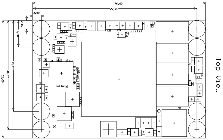
- Xilinx ZYNQ UltraScale+ XCZU9EG ZU7EV-1FBVB900 MPSoC, U1
- EN63A0QI 12A PowerSoC DC-DC converter, U4
- TI TPS72018 LDO @1.8V, U6
- TI TPS74401 LDO @0.9V, U14
- TI TPS74401 LDO @1.2V, U28
- TI TPS72018 LDO @1.8V, U6
- Quarz Crystal @50.000MHz, Y1
- Low-power programmable oscillator @ 3325.333333 000000 MHz (PS_CLKIN0 for U5), U32
- Red LED (DONE), D1
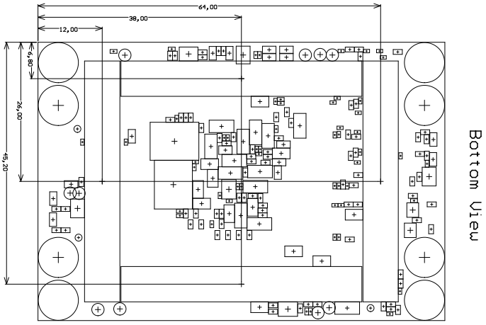
- U25
- TI TPS74801 LDO @1.8V, U10
- TI TPS74801 LDO @0.9V, U8
- 8 Gbit (512Mx16) 256Mx16 DDR4-2400 SDRAM, U12
- 256Mx16 8 Gbit (512Mx16) DDR4-2400 SDRAM, U9
- 256Mx16 8 Gbit (512Mx16) DDR4-2400 SDRAM, U2
- 256Mx16 8 Gbit (512Mx16) DDR4-2400 SDRAM, U312A PowerSoC DC-DC converter, U4
- Quartz crystal, Y1
- Low-power programmable oscillator @ 25.000000 MHz (IN0 for U5), U25
- 10-channel programmable PLL clock generator, U5
- Ultra fine 0.50 mm pitch, Razor Beam™ LP Slim Terminal Strip with 160 contacts, J4J3
- Ultra fine 0.50 mm pitch, Razor Beam™ LP Slim Terminal Strip with 160 contacts, J2J1
- Ultra fine 0.50 mm pitch, Razor Beam™ LP Slim Terminal Strip with 160 contacts, J3J4
- Ultra fine 0.50 mm pitch, Razor Beam™ LP Slim Terminal Strip with 160 contacts, J1
- Quartz crystal, Y2
- 256 Mbit serial NOR Flash memory, U7
- J2
- 1.8V, 512 Mbit QSPI flash memory ,U17
- 1.8V, 512 Mbit QSPI flash memory, U7
- TI TPS72018 LDO @1.8V, U27256 Mbit serial NOR Flash memory, U17
Initial Delivery State
| Storage Device Name | Content | Notes |
|---|---|---|
SPI Flash OTP Area | Empty, not programmed | Except serial number programmed by flash vendor. |
SPI Flash Quad Enable bit | Programmed | - |
SPI Flash main array | Not programmed | - |
eFUSE USER | Not programmed | - |
eFUSE Security | Not programmed | - |
| Si5345A OTP NVM | Not programmed | - |
...
| Bank | Type | Lane | Signal Name | B2B Pin | FPGA Pin | ||||||||||
|---|---|---|---|---|---|---|---|---|---|---|---|---|---|---|---|
| 228224 | GTH | 0 |
|
|
| ||||||||||
| 1 | 2 |
| 3 | 229 | GTH | 0 |
|
|
| ||||||
| 2 | 3 | 230 | GTH | 0 |
|
|
| 1 | 2
| ||||||
| 3 | 128 | GTH | 0 |
|
|
| 1 | 2 | 3 | 505 | GTR | 0 | 1 | 2 | 3 |
Table 4: MGT lanes
There are 3 clock sources for the GTR transceivers. B505_CLK0 is connected directly to B2B connector JM3, so the clock can be provided by the carrier board. Clocks B505_CLK1 and B505_CLK3 are provided by the on-board clock generator (U10). As there are no capacitive coupling of the data and clock lines that are connected to the connectors, these may be required on the user’s PCB depending on the application.
...
Table 5: MGT reference clock sources
JTAG Interface
JTAG access is provided through the MPSoC's PS configuration bank 503 with bank voltage PS_1V8.
...
Table 4: B2B connector pin-out of JTAG interface.
Configuration Bank Control Signals
The Xilinx Zynq UltraScale+ MPSoC's PS configuration bank 503 control signal pins are accessible through B2B connector J2.
For further information about the particular control signals and how to use and evaluate them, refer to the Xilinx Zynq UltraScale+ MPSoC TRM and UltraScale Architecture Configuration - User Guide.
...
4-bit boot mode pins.
For further information about the boot modes refer to the Xilinx Zynq UltraScale+ MPSoC TRM section 'Boot and Configuration'.
...
ERR_OUT signal is asserted for accidental loss of power, an error, or an exception in the MPSoC's Platform Management Unit (PMU).
ERR_STATUS indicates a secure lock-down state.
...
| |||||
| 225 | GTH | 0 |
|
|
|
| 1 |
|
|
| ||
| 2 |
|
|
| ||
| 3 |
|
|
| ||
| 226 | GTH | 0 |
|
|
|
| 1 |
|
|
| ||
| 2 |
|
|
| ||
| 3 |
|
|
| ||
| 227 | GTH | 0 |
|
|
|
| 1 |
|
|
| ||
| 2 |
|
|
| ||
| 3 |
|
|
| ||
| 505 | GTR | 0 |
|
|
|
| 1 |
|
|
| ||
| 2 |
|
|
| ||
| 3 |
|
|
|
Table 4: MGT lanes
There are 2 clock sources for the GTH and GTR transceivers. The clock inputs of the MGT transceivers are connected directly to the B2B connectors, so the clock can be provided by the carrier board, and clock inputs are also provided by the on-board clock generator Si5345A (U5). As there are no capacitive coupling of the data and clock lines that are connected to the B2B connectors, these may be required on the user’s PCB depending on the application.
| Clock signal | Bank | Source | FPGA Pin | Notes |
|---|---|---|---|---|
| B224_CLK0_P | 224 | B2B, J3-62 | MGTREFCLK0P_224, R8 | Supplied by the carrier board |
| B224_CLK0_N | 224 | B2B, J3-60 | MGTREFCLK0N_224, R7 | Supplied by the carrier board |
| B224_CLK1_P | 224 | U5, CLK4_P | MGTREFCLK1P_224, N8 | On-board Si5345A |
| B224_CLK1_N | 224 | U5, CLK4_N | MGTREFCLK1N_224, N7 | On-board Si5345A |
| B225_CLK0_P | 225 | B2B, J3-67 | MGTREFCLK0P_225, L8 | Supplied by the carrier board |
| B225_CLK0_N | 225 | B2B, J2-65 | MGTREFCLK0N_225, L7 | Supplied by the carrier board |
| B225_CLK1_P | 225 | U5, CLK3_P | MGTREFCLK1P_225, J8 | On-board Si5345A |
| B225_CLK1_N | 225 | U5, CLK3_N | MGTREFCLK1N_225, J7 | On-board Si5345A |
| B226_CLK0_P | 226 | U5, CLK2_P | MGTREFCLK0P_226, H10 | On-board Si5345A |
| B226_CLK0_N | 226 | U5, CLK2_N | MGTREFCLK0N_226, H9 | On-board Si5345A |
| B226_CLK1_P | 226 | B2B, J3-61 | MGTREFCLK1P_226, F10 | Supplied by the carrier board |
| B226_CLK1_N | 226 | B2B, J3-59 | MGTREFCLK1N_226, F9 | Supplied by the carrier board |
| B227_CLK0_P | 227 | U5, CLK1_P | MGTREFCLK0P_227, D10 | On-board Si5345A |
| B227_CLK0_N | 227 | U5, CLK1_N | MGTREFCLK0N_227, D9 | On-board Si5345A |
| B227_CLK1_P | 227 | B2B, J2-22 | MGTREFCLK1P_227, B10 | Supplied by the carrier board |
| B227_CLK1_N | 227 | B2B, J2-24 | MGTREFCLK1N_227, B9 | Supplied by the carrier board |
| B505_CLK0_P | 505 | B2B, J2-10 | PS_MGTREFCLK0P_505, M23 | Supplied by the carrier board |
| B505_CLK0_N | 505 | B2B, J2-12 | PS_MGTREFCLK0N_505, M24 | Supplied by the carrier board |
| B505_CLK1_P | 505 | B2B, J2-16 | PS_MGTREFCLK1P_505, L25 | Supplied by the carrier board |
| B505_CLK1_N | 505 | B2B, J2-18 | PS_MGTREFCLK1N_505, L26 | Supplied by the carrier board |
| B505_CLK2_P | 505 | U5, CLK5_P | PS_MGTREFCLK2P_505, K23 | On-board Si5345A |
| B505_CLK2_N | 505 | U5, CLK5_N | PS_MGTREFCLK2N_505, K24 | On-board Si5345A |
| B505_CLK3_P | 505 | U5, CLK6_P | PS_MGTREFCLK3P_505, H23 | On-board Si5345A |
| B505_CLK3_N | 505 | U5, CLK6_N | PS_MGTREFCLK3N_505, H24 | On-board Si5345A |
Table 5: MGT reference clock sources
JTAG Interface
JTAG access is provided through the MPSoC's PS configuration bank 503 with bank voltage PS_1V8.
| JTAG Signal | B2B Connector Pin |
|---|---|
| TCK | J2-120 |
| TDI | J2-122 |
| TDO | J2-124 |
| TMS | J2-126 |
Table 4: B2B connector pin-out of JTAG interface.
Configuration Bank Control Signals
The Xilinx Zynq UltraScale+ MPSoC's PS configuration bank 503 control signal pins are accessible through B2B connector J2.
For further information about the particular control signals and how to use and evaluate them, refer to the Xilinx Zynq UltraScale+ MPSoC TRM and UltraScale Architecture Configuration - User Guide.
| Signal | B2B Connector Pin | Function |
|---|---|---|
| DONE | J2-116 | PL configuration completed. |
| PROG_B | J2-100 | PL configuration reset signal. |
| INIT_B | J2-98 | PS is initialized after a power-on reset. |
| SRST_B | J2-96 | System reset. |
| MODE0 ... MODE3 | J2-109/J2-107/J2-105/J2-103 | 4-bit boot mode pins. For further information about the boot modes refer to the Xilinx Zynq UltraScale+ MPSoC TRM section 'Boot and Configuration'. |
| ERR_STATUS / ERR_OUT | J2-86 / J2-88 | ERR_OUT signal is asserted for accidental loss of power, an error, or an exception in the MPSoC's Platform Management Unit (PMU). ERR_STATUS indicates a secure lock-down state. |
| PUDC_B | J2-127 | Pull-up during configuration (pulled-up to PL_1V8). |
Table 5: B2B connector pin-out of MPSoC's PS configuration bank.
Analog Input
The Xilinx Zynq UltraScale+ MPSoC provides differential pairs for analog input values. The pins are exposed to B2B-connector J2.
| Signal | B2B Connector Pin | Function |
|---|---|---|
| V_P, V_N | J2-113, J2-115 | System Monitor |
| DX_P, DX_N | J2-119, J2-121 | Temperature-sensing diode pins |
Table 6: B2B connector pin-out of analog input pins
Quad SPI Interface
Quad SPI Flash memory ICs U7 and U17 are connected to the Zynq MPSoC PS QSPI0 interface via PS MIO bank 500, pins MIO0 ... MIO5 and MIO7 ... MIO12.
| MIO | Signal Name | U7 Pin | MIO | Signal Name | U17 Pin | |
|---|---|---|---|---|---|---|
| 0 | SPI Flash CLK | B2 | 7 | SPI Flash CS | C2 | |
| 1 | SPI Flash IO1 | D2 | 8 | SPI Flash IO0 | D3 | |
| 2 | SPI Flash IO2 | C4 | 9 | SPI Flash IO1 | D2 | |
| 3 | SPI Flash IO3 | D4 | 10 | SPI Flash IO2 | C4 | |
| 4 | SPI Flash IO0 | D3 | 11 | SPI Flash IO3 | D4 | |
| 5 | SPI Flash CS | C2 | 12 | SPI Flash CLK | B2 |
Table 7: PS MIO pin assignment of the Quad SPI Flash memory ICs.
Default PS MIO Mapping
| PS MIO | Function | Connected to |
|---|---|---|
| 0 | SPI0 | U7-B2, CLK |
| 1 | SPI0 | U7-D2, DO/IO1 |
| 2 | SPI0 | U7-C4, WP/IO2 |
| 3 | SPI0 | U7-D4, HOLD/IO3 |
| 4 | SPI0 | U7-D3, DI/IO0 |
| 5 | SPI0 | U7-C2, CS |
| 6 | N/A | Not connected |
| 7 | SPI1 | U17-C2, CS |
| 8 | SPI1 | U17-D3, DI/IO0 |
| 9 | SPI1 | U17-D2, DO/IO1 |
| 10 | SPI1 | U17-C4, WP/IO2 |
| 11 | SPI1 | U17-D4, HOLD/IO3 |
| 12 | SPI1 | U17-B2, CLK |
| 13..20 | eMMC | U6, MMC-D0..D7 |
| 33 | MIO | B2B |
| 34..37 | - | Not connected |
| 38 | I2C | U10-12, SCL |
| 39 | I2C | U10-19, SDA |
Table 5: B2B connector pin-out of MPSoC's PS configuration bank.
Analog Input
The Xilinx Zynq UltraScale+ MPSoC provides differential pairs for analog input values. The pins are exposed to B2B-connector J2.
...
Table 6: B2B connector pin-out of analog input pins
Quad SPI Interface
Quad SPI Flash memory ICs U7 and U17 are connected to the Zynq MPSoC PS QSPI0 interface via PS MIO bank 500, pins MIO0 ... MIO5 and MIO7 ... MIO12.
...
Table 7: PS MIO pin assignment of the Quad SPI Flash memory ICs.
Default PS MIO Mapping
...
JM1-19
...
JM1-21
...
63
...
Table 8: TE0807-01 PS MIO mapping
...
| Scroll Title | ||||
|---|---|---|---|---|
| ||||
|
Revision History
Hardware Revision History
| Date | Revision | Notes | PCN Link | Documentation Link |
|---|---|---|---|---|
| - | 0102 | current available module revision | - | TE0807-02 |
| - | 01 | first production release | - | TE0807-01 |
Table 20: Hardware revision history table
...
Overview
Content Tools