Page History
...
| Scroll Title | ||||||||||||||||||||||||||||||||
|---|---|---|---|---|---|---|---|---|---|---|---|---|---|---|---|---|---|---|---|---|---|---|---|---|---|---|---|---|---|---|---|---|
| ||||||||||||||||||||||||||||||||
|
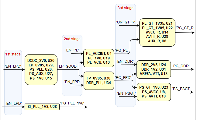
Operation Conditions of the DC-DC Converter Control Signals
...
| Scroll Title | ||||||||||||||||||||||||
|---|---|---|---|---|---|---|---|---|---|---|---|---|---|---|---|---|---|---|---|---|---|---|---|---|
| ||||||||||||||||||||||||
|
Power Rails
Power Rail Name | B2B J1 Pins | B2B J2 Pins | B2B J3 Pins | B2B J4 Pins | Directions | Note |
|---|---|---|---|---|---|---|
| PL_DCIN | 151, 153, 157, 159 | - | - | - | Input | - |
| DCDCIN | - | 154, 156, 158, 160, | - | - | Input | - |
| LP_DCDC | - | 138, 140, 142, 144 | - | - | Input | - |
| PS_BATT | - | 125 | - | - | Input | - |
| GT_DCDC | - | - | 157, 158, 159, 160 | - | Input | - |
| PLL_3V3 | - | - | 152 | - | Input | U5 (programmable PLL) 3.3V nominal input |
| SI_PLL_1V8 | - | - | 151 | - | Output | Internal voltage level 1.8V nominal output |
| PS_1V8 | - | 99 | 147, 148 | - | Output | Internal voltage level |
| PL_1V8 | 91, 121 | - | - | - | Output | Internal voltage level |
| DDR_1V2 | - | 135 | - | - | Output | Internal voltage level |
| VCCO47 | - | - | 43, 44 | - | Input | - |
| VCCO48 | - | - | 15, 16 | - | Input | - |
| VCCO64 | - | - | - | 58, 106 | Input | - |
| VCCO65 | - | - | - | 69, 105 | Input | - |
| VCCO66 | 90, 120 | - | - | - | Input | - |
Table 1617: TE0807-02 power rails
Bank Voltages
| Bank | Type | Schematic Name | Voltage | Reference Input Voltage | Voltage Range |
|---|---|---|---|---|---|
| 47 | HD | VCCO47 | user | - | 1.2V to 3.3V |
| 48 | HD | VCCO48 | user | - | 1.2V to 3.3V |
| 64 | HP | VCCO64 | user | VREF_64, pin J4-88 | 1.2V to 1.8V |
| 65 | HP | VCCO65 | user | VREF_65, pin J4-15 | 1.2V to 1.8V |
| 66 | HP | VCCO66 | user | VREF_66, pin J1-108 | 1.2V to 1.8V |
| 500 | MIO | PS_1V8 | 1.8V | - | - |
| 501 | MIO | PS_1V8 | 1.8V | - | - |
| 502 | MIO | PS_1V8 | 1.8V | - | - |
| 503 | CONFIG | PS_1V8 | 1.8V | - | - |
Table 1718: TE0807-02 I/O bank voltages
...
Parameter | Min | Max | Unit | Notes / Reference Document |
|---|---|---|---|---|
| PL_DCIN | -0.3 | 7 | V | TPS82085SIL / EN63A0QI data sheet |
| DCDCIN | -0.3 | 7 | V | TPS82085SIL / TPS51206 data sheet |
| LP_DCDC | -0.3 | 4 | V | TPS3106K33DBVR data sheet |
| GT_DCDC | -0.3 | 7 | V | TPS82085SIL data sheet |
| PS_BATT | -0.5 | 2 | V | Xilinx DS925 data sheet |
| PLL_3V3 | -0.5 | 3.8 | V | Si5345/44/42 data sheet |
| VCCO for HD I/O banks | -0.5 | 3.4 | V | Xilinx DS925 data sheet |
| VCCO for HP I/O banks | -0.5 | 2 | V | Xilinx DS925 data sheet |
| VREF | -0.5 | 2 | V | Xilinx DS925 data sheet |
| I/O input voltage for HD I/O banks | -0.55 | VCCO + 0.55 | V | Xilinx DS925 data sheet |
| I/O input voltage for HP I/O banks | -0.55 | VCCO + 0.55 | V | Xilinx DS925 data sheet |
| PS I/O input voltage (MIO pins) | -0.5 | VCCO_PSIO + 0.55 | V | Xilinx DS925 data sheet, VCCO_PSIO 1.8V nominally |
Receiver (RXP/RXN) and transmitter | -0.5 | 1.2 | V | Xilinx DS925 data sheet |
Voltage on input pins of | -0.5 | VCC + 0.5 | V | NC7S08P5X data sheet, see schematic for VCC |
Voltage on input pins (nMR) of | -0.3 | VDD + 0.3 | V | TPS3106 data sheet, |
| "Enable"-signals on TPS82085SIL (EN_PLL_PWR, EN_LPD) | -0.3 | 7 | V | TPS82085SIL data sheet |
Storage temperature (ambient) | -40 | 100 | °C | ROHM Semiconductor SML-P11 Series data sheet |
Table 1819: Module absolute maximum ratings
...
| Parameter | Min | Max | Unit | Notes / Reference Document |
|---|---|---|---|---|
| PL_DCIN | 23.53 | 6 | V | EN63A0QI / TPS82085SIL data sheet |
| DCDCIN | 3.13 | 6 | V | TPS82085SIL / TPS51206PSQ data sheet |
| LP_DCDC | 23.53 | 3.6 | V | TPS82085SIL / TPS3106 data sheet |
| GT_DCDC | 23.53 | 6 | V | TPS82085SIL data sheet |
| PS_BATT | 1.2 | 1.5 | V | Xilinx DS925 data sheet |
| PLL_3V3 | 3.143 | 3.47 | V | Si5345/44/42 data sheet 3.3V typical |
| VCCO for HD I/O banks | 1.14 | 3.4 | V | Xilinx DS925 data sheet |
| VCCO for HP I/O banks | 0.95 | 1.9 | V | Xilinx DS925 data sheet |
| I/O input voltage for HD I/O banks. | -0.2 | VCCO + 0.2 | V | Xilinx DS925 data sheet |
| I/O input voltage for HP I/O banks | -0.2 | VCCO + 0.2 | V | Xilinx DS925 data sheet |
| PS I/O input voltage (MIO pins) | -0.2 | VCCO_PSIO + 0.2 | V | Xilinx DS925 data sheet, VCCO_PSIO 1.8V nominally |
| Voltage on input pins of NC7S08P5X 2-Input AND Gate | 0 | VCC | V | NC7S08P5X data sheet, |
Voltage on input pin 'MR' of | 0 | VDD | V | TPS3106 data sheet, |
Table 1920: Recommended operating conditions
...
| Date | Revision | Notes | PCN Link | Documentation Link |
|---|---|---|---|---|
| - | 02 | current available module revision | - | TE0807-02 |
| - | 01 | first production release | - | TE0807-01 |
Table 2021: Hardware revision history table
...
| Scroll Title | ||||
|---|---|---|---|---|
| ||||
|
Document Change History
| HTML |
|---|
<!-- Generate new entry: 1.add new row below first 2.Copy "Page Information Macro(date)" Macro-Preview, Metadata Version number, Author Name and description to the empty row. Important Revision number must be the same as the Wiki document revision number 3.Update Metadata = "Page Information Macro (current-version)" Preview+1 and add Author and change description. --> |
...
Overview
Content Tools