Page History
...
| Scroll Title | ||||||||||||||||||||||||||||||||
|---|---|---|---|---|---|---|---|---|---|---|---|---|---|---|---|---|---|---|---|---|---|---|---|---|---|---|---|---|---|---|---|---|
| ||||||||||||||||||||||||||||||||
|
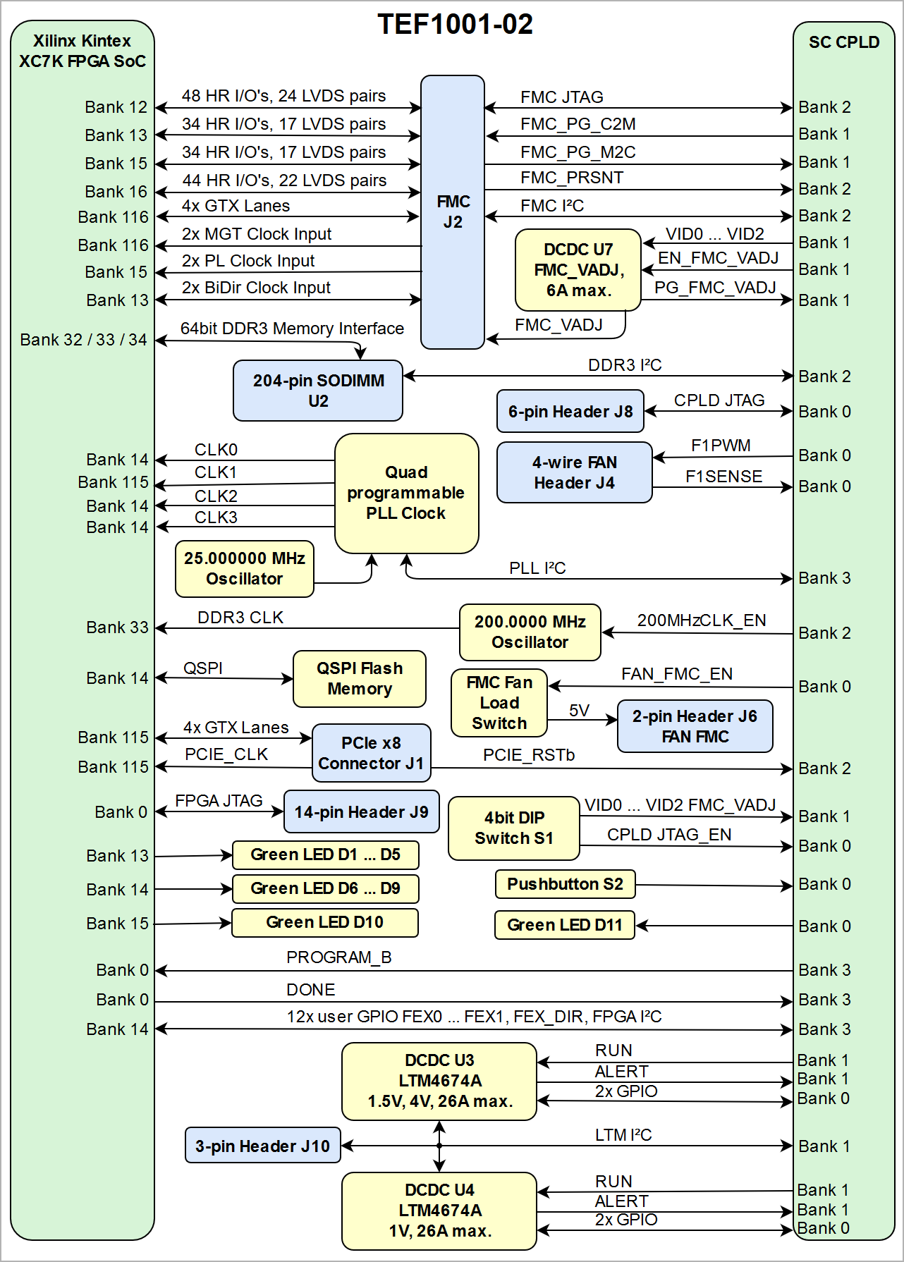
Main Components
...
| HTML |
|---|
<!-- Connections and Interfaces or B2B Pin's which are accessible by User --> |
FMC HPC Connector
...
I/O signals connected to the SoCs I/O bank and FMC connector J2:
...
Table 2: General overview of FPGA's PL I/O signals connected to the FMC connector
| I²C Interface | Schematic net names | Connected to | I²C Address | Notes |
|---|---|---|---|---|
| FMC Connector, J2 | 'FMC_SDA', pin C31 | SC CPLD U5, pin 48 | 0x50 | - |
For detailed information about the pin out, please refer to the Pin-out Tables.
...
Table 5: JTAG interface signals
System Controller CPLD I/O Pins
Special purpose pins are connected to the System Controller CPLD and have following default configuration:
FAN Connectors
The TEF1001 board offers two FAN connectors for cooling the FPGA device and on built-in FAN for the FMC modules.
| Connector | Schematic net names | Connected to | Notes |
|---|---|---|---|
| 4-Wire PWM FAN connector J4, 12V power supply | 'F1SENSE', pin 3 | SC CPLD U5, pin 99 | FPGA cooling FAN can be controlled via I²C interface from FPGA, see current SC CPLD firmware |
| 2-pin FAN connector J6, 5V power supply with TPS2051 Load Switch U25 | 'FAN_FMC_EN', U25 pin 4 | SC CPLD U5, pin 78 | FMC cooling FAN |
Table 9: FAN connectors
On-board Peripherals
| HTML |
|---|
<!--
Components on the Module, like Flash, PLL, PHY...
--> |
System Controller CPLD
The System Controller CPLD (U5) is provided by Lattice Semiconductor LCMXO2-256HC (MachXO2 Product Family). The SC-CPLD is the central system management unit where essential control signals are logically linked by the implemented logic in CPLD firmware, which generates output signals to control the system, the on-board peripherals and the interfaces. Interfaces like JTAG and I2C between the on-board peripherals and to the FPGA module are by-passed, forwarded and controlled by the System Controller CPLD.
Other tasks of the System Controller CPLD are the monitoring of the power-on sequence and to display the programming state of the FPGA module.
For detailed information, refer to the reference page of the SC CPLD firmware of this module. Table below lists the SC CPLD I/O pins with their default configuration:
| Pin Name | SC CPLD Direction | Function | Default Configuration |
|---|---|---|---|
| 200MHZCLK_EN | out | control line | enables 200.0000MHz oscillator U1 |
| BUTTON | in | user | Reset Button |
| CPLD_TDO | out | CPLD JTAG interface | - |
| CPLD_TDI | in | ||
| CPLD_TCK | in | ||
| CPLD_TMS | in | ||
| JTAG_EN | in | ||
| DDR3_SCL | in / out | I²C bus of DDR3 SODIMM socket | I²C connected to FPGA |
| DDR3_SDA | in / out | ||
| PLL_SCL | in / out | I²C bus of SI5338 quad clock PLL | I²C connected to FPGA |
| PLL_SDA | in / out | ||
| PCIE_RSTB | in | PCIe reset input | see current SC CPLD firmware |
| FEX_DIR / FEX0 ... FEX11 | in / out | user GPIO | see current SC CPLD firmware |
| F1PWM | out | FPGA FAN control | see current SC CPLD firmware |
| F1SENSE | in | ||
| FAN_FMC_EN | out | FMC FAN enable | |
| FMC_PG_C2M | out | FMC signals and pins | see current SC CPLD firmware |
| FMC_PG_M2C | in |
| FMC_PRSNT_M2C_L | in | ||
| FMC_SCL | in / out | FMC I²C | I²C connected to FPGA |
| FMC_SDA | in / out | ||
| FMC_TCK | FMC JTAG | see current SC CPLD firmware | |
| FMC_TDI | |||
| FMC_TDO | |||
| FMC_TMS | |||
| FMC_TRST | |||
| DONE | in | FPGA configuration signal | PL configuration completed |
| PROGRAM_B | out | PL configuration reset signal | |
| LED1 | out | LED status signal | see current CPLD firmware |
| FPGA_IIC_OE | in |
SC CPLD
| SC CPLD works as I²C switch with the FPGA as I²C-Master and on-board peripherals as I²C-slaves | I²C output enable, connected to PL bank 14 pin F25 | ||
| FPGA_IIC_SCL | in / out | I²C clock line, connected to PL bank 14 pin G26 | |
| FPGA_IIC_SDA | in / out | I²C data line, connected to PL bank 14 pin G25 | |
| EN_1V8 | out | Power control | enable signal DCDC U20 '1V8' |
| PG_1V8 | in | power good signal DCDC U20 '1V8' | |
| EN_3V3FMC | out | enable signal DCDC U15 'EN_3V3FMC' | |
| PG_3V3 | in | power good signal U15 'EN_3V3FMC' | |
| EN_FMC_VADJ | out | enable signal DCDC U7 'FMC_VADJ' | |
| PG_FMC_VADJ | in | power good DCDC U7 'FMC_VADJ' | |
VID0_FMC_VADJ, | out | DCDC U7 power selection pin | |
VID0_FMC_VADJ_CTRL, | in | Power selection of FMC_VADJ, forwarded to DCDC U7 | |
| LTM_1V5_RUN | out | enable signals of DCDC U3, U4 (LTM4676) see current CPLD firmware | |
| LTM_4V_RUN | out | ||
| LTM_SCL | in / out | DCDC U3, U4 (LTM4676) I²C | I²C connected to FPGA |
| LTM_SDA | in / out | ||
| LTM1_ALERT | in | DCDC U3, U4 (LTM4676) control | see current CPLD firmware |
| LTM2_ALERT | in | ||
| LTM_1V_IO0 | in / out | ||
| LTM_1V_IO1 | in / out | ||
| LTM_1V5_4V_IO0 | in / out | ||
| LTM_1V5_4V_IO1 | in / out |
Table 6: System Controller CPLD I/O pins
...
| HTML |
|---|
<!-- For the detailed function of the pins and signals, the internal signal assignment and implemented logic, look to the Wiki reference page SC CPLD of this module or into the bitstream filefile of the SC CPLD. Add link to the Wiki reference page of the SC CPLD, if available. Add --> |
| HTML |
|---|
<!-- Put in link to the Wiki reference page of the firmware of the SC CPLD, if available. --> |
Quad SPI Interface
Quad SPI Flash memory interface is connected to the FPGA bank 14, QSPI clock is provided by FPGA config bank 0.
...
Table 7: Quad SPI interface signals and connections
I2C Interface
On-module I²C interface is routed from PL bank 14 I/O pins (FPGA_IIC_SDA, FPGA_IIC_SCL and FPGA_IIC_OE) to the I²C interface of SC CPLD U5 which works as I²C switch with the FPGA as I²C-Master. The I²C interfaces of the on-board peripherals are muxed to the FPGA I²C interface via SC CPLD U5. Also the FAN control of the 4-wire PWM FAN connector J4 can be controlled via I²C from FPGA. For detailed information, refer to the reference page of the SC CPLD firmware of this module, section I²C.
...
'FPGA_IIC_SDA', pin G25
'FPGA_IIC_SCL', pin G26
'FPGA_IIC_OE', pin F25
...
SC CPLD U5, pin 16
SC CPLD U5, pin 1
SC CPLD U5, pin 14
...
'PLL_SDA', pin 19
'PLL_SCL', pin 12
...
SC CPLD U5, pin 8
SC CPLD U5, pin 2
...
'LTM_SDA', pin D6
'LTM_SCL', pin E6
...
SC CPLD U5, pin 66
SC CPLD U5, pin 67
...
'DDR3_SDA', pin 200
'DDR3_SCL', pin 202
...
SC CPLD U5, pin 42
SC CPLD U5, pin 43
...
'FMC_SDA', pin C31
'FMC_SCL', pin C30
...
SC CPLD U5, pin 48
SC CPLD U5, pin 49
...
Table 8: I2C slave device addresses
FAN Connectors
The TEF1001 board offers two FAN connectors for cooling the FPGA device and on built-in FAN for the FMC modules.
...
'F1SENSE', pin 3
'F1PWM', pin 4
...
SC CPLD U5, pin 99
SC CPLD U5, pin 98
...
'FAN_FMC_EN', U25 pin 4
...
SC CPLD U5, pin 78
...
Table 9: FAN connectors
On-board Peripherals
| HTML |
|---|
<!--
Components on the Module, like Flash, PLL, PHY...
--> |
System Controller CPLD
The System Controller CPLD (U5) is provided by Lattice Semiconductor LCMXO2-256HC (MachXO2 Product Family). The SC-CPLD is the central system management unit where essential control signals are logically linked by the implemented logic in CPLD firmware, which generates output signals to control the system, the on-board peripherals and the interfaces. Interfaces like JTAG and I2C between the on-board peripherals and to the FPGA module are by-passed, forwarded and controlled by the System Controller CPLD.
Other tasks of the System Controller CPLD are the monitoring of the power-on sequence and to display the programming state of the FPGA module.
For detailed information, refer to the reference page of the SC CPLD firmware of this module.
| HTML |
|---|
<!--
Put in link to the Wiki reference page of the firmware of the SC CPLD.
--> |
DDR3 SDRAM SODIMM Socket
The TEF1001 board supports additional DDR3 SODIMM via 204-pin socket U2. The DDR3 memory interface has a 64bit wide databus and is routed to the FPGA banks 32, 33 and 34.
The reference clock signal for the DDR3 interface is generated by the 200.0000MHz MEMS oscillator U1 and is applied to the FPGA bank 33.
There is also a I2C interface between the System Controller CPLD U5 and the DDR3 SODIMM memory socket U2.
Quad SPI Flash Memory
A 256 Mbit (32 MByte) Quad SPI Flash Memory (Micron N25Q256A, U12) is provided for FPGA configuration file storage. After configuration process completes the remaining free memory can be used for application data storage. All four SPI data lines are connected to the FPGA allowing x1, x2 or x4 data bus widths to be used. The maximum data transfer rate depends on the bus width and clock frequency. The memory can be accessed indirectly by the FPGA JTAG port (J9) by implementing the functional logic for this purpose inside the FPGA.
| Note |
|---|
SPI Flash QE (Quad Enable) bit must be set to high or FPGA is unable to load its configuration from flash during power-on. By default this bit is set to high at the manufacturing plant. |
Programmable Clock Generator
There is a Silicon Labs I2C programmable quad PLL clock generator on-board (Si5338A, U13) to generate various reference clocks for the module.
...
IN1
...
-
...
not used
...
IN3
...
Reference input clock
...
IN4
...
IN5
...
-
...
CLK0A
...
CLK0_P
...
Clock to PL bank 14
...
Clock to MGT bank 115,
AC decoupled
...
CLK2_P
...
Table 10: Programmable quad PLL clock generator inputs and outputs
Oscillators
The FPGA module has following reference clocking sources provided by on-board oscillators and FMC connector J2:
...
Enable by SC CPLD U5, pin 30
Signal: '200MHzCLK_EN'
...
DDR3 SDRAM SODIMM Socket
The TEF1001 board supports additional DDR3 SODIMM via 204-pin socket U2. The DDR3 memory interface has a 64bit wide databus and is routed to the FPGA banks 32, 33 and 34.
The reference clock signal for the DDR3 interface is generated by the 200.0000MHz MEMS oscillator U1 and is applied to the FPGA bank 33.
There is also a I2C interface between the System Controller CPLD U5 and the DDR3 SODIMM memory socket U2.
| I²C Interface | Schematic net names | Connected to | I²C Address | Notes |
|---|---|---|---|---|
| DDR3 SODIMM, U2 | 'DDR3_SDA', pin 200 | SC CPLD U5, pin 42 | module dependent | - |
Table 8: DDR3 SODIMM socket I²C interface
Quad SPI Flash Memory
A 256 Mbit (32 MByte) Quad SPI Flash Memory (Micron N25Q256A, U12) is provided for FPGA configuration file storage. After configuration process completes the remaining free memory can be used for application data storage. All four SPI data lines are connected to the FPGA allowing x1, x2 or x4 data bus widths to be used. The maximum data transfer rate depends on the bus width and clock frequency. The memory can be accessed indirectly by the FPGA JTAG port (J9) by implementing the functional logic for this purpose inside the FPGA.
Quad SPI Flash memory interface is connected to the FPGA bank 14, QSPI clock is provided by FPGA config bank 0.
| Signal Name | QSPI Flash Memory U12 Pin | FPGA Pin |
|---|---|---|
| FLASH_QSPI_CS | S, Pin 7 | Bank 14, Pin C23 |
| FLASH_QSPI_D00 | DQ0, Pin 15 | Bank 14, Pin B24 |
| FLASH_QSPI_D01 | DQ1, Pin 8 | Bank 14, Pin A25 |
| FLASH_QSPI_D02 | DQ2, Pin 9 | Bank 14, Pin B22 |
| FLASH_QSPI_D03 | DQ3, Pin 1 | Bank 14, Pin A22 |
| FPGA_CFG_CCLK | C, Pin 16 | Bank 0, Pin C8 |
Table 7: Quad SPI interface signals and connections
| Note |
|---|
SPI Flash QE (Quad Enable) bit must be set to high or FPGA is unable to load its configuration from flash during power-on. By default this bit is set to high at the manufacturing plant. |
Programmable Clock Generator
There is a Silicon Labs I2C programmable quad PLL clock generator on-board (Si5338A, U13) to generate various reference clocks for the module.
| Si5338A Pin | Signal Name / Description | Connected to | Direction | Note |
|---|---|---|---|---|
IN1 | - | not connected | Input | not used |
| IN2 | - | GND | Input | not used |
IN3 | Reference input clock | U3, pin 3 | Input | 25.000000 MHz oscillator U14, Si8208AI |
IN4 | - | GND | Input | I2C slave device address LSB |
IN5 | - | not connected | Input | not used |
| IN6 | - | GND | Input | not used |
| SCL | PLL_SCL | SC CPLD U5, pin 8 | Input / Output | I²C interface muxed to FPGA Slave address: 0x70. |
| SDA | PLL_SDA | SC CPLD U5, pin 2 | Input / Output | |
CLK0A | CLK0_P | U6, G24 | Output | Clock to PL bank 14 |
| CLK0B | CLK0_N | U6, F24 | ||
| CLK1A | MGTCLK_5338_P | U6, H6 | Output | Clock to MGT bank 115, |
| CLK1B | MGTCLK_5338_N | U6, H5 | ||
| CLK2A | CLK1_P | U6, G22 | Output | Clock to PL bank 14 |
| CLK2B | CLK1_N | U6, F23 | ||
| CLK3A | CLK2_P | U6, D23 | Output | Clock to PL bank 14 |
| CLK3B | CLK2_N | U6, D24 |
Table 10: Programmable quad PLL clock generator inputs and outputs
Oscillators
The FPGA module has following reference clocking sources provided by on-board oscillators and FMC connector J2:
| Clock Source | Frequency | Signal Schematic Name | Clock Destination | Notes |
|---|---|---|---|---|
| U14, SiT8208AI | 25.000000 MHz | CLK | Si5338A PLL U13, pin 3 (IN3) | - |
| U1, DSC1123DL5 | 200.0000 MHz | DDR3_CLK_P | FPGA bank 33, pin AB11 | Enable by SC CPLD U5, pin 30 Signal: '200MHzCLK_EN' |
| DDR3_CLK_N | FPGA bank 33, pin AC11 | |||
| FMC Connector J2 | - | GBTCLK0_M2C_P, Pin J2-D4 | FPGA bank 116, pin D6 | reference clock to MGT bank 116 |
| GBTCLK0_M2C_N, Pin J2-D5 | FPGA bank 116, pin D5 | |||
| - | GBTCLK1_M2C_P, Pin J2-B20 | FPGA bank 116, pin F6 | reference clock to MGT bank 116 | |
| GBTCLK1_M2C_N, Pin J2-B21 | FPGA bank 116, pin F5 | |||
| - | CLK0_M2C_P, Pin J2-H4 | FPGA bank 15, pin H17 | reference clock to PL bank 15 | |
| CLK0_M2C_N, Pin J2-H5 | FPGA bank 15, pin H18 | |||
| - | CLK1_M2C_P, Pin J2-G2 | FPGA bank 15, pin G17 | reference clock to PL bank 15 | |
| CLK1_M2C_N, Pin J2-G3 | FPGA bank 15, pin G18 | |||
| - | CLK2_BIDIR_P, Pin J2-K4 | FPGA bank 13, pin P23 | reference clock to PL bank 13 bidirectional clock line | |
| CLK2_BIDIR_N, Pin J2-K5 | FPGA bank 13, pin N23 | |||
| - | CLK3_BIDIR_P, Pin J2-J2 | FPGA bank 13, pin R22 | reference clock to PL bank 13 bidirectional clock line | |
| CLK3_BIDIR_N, Pin J2-J3 | FPGA bank 13, pin R23 |
Table 11: Reference clock signals
On-board LEDs
| LED | Color | Signal Schematic name | Connected to | Description and Notes |
|---|---|---|---|---|
| D1 | Green | FPGA_LED1_VT | FPGA bank 13, pin K25 | LEDs D1 to D10 are available to user. LED voltages are translated from bank voltage |
| D2 | Green | FPGA_LED2_VT | FPGA bank 13, pin K26 | |
| D3 | Green | FPGA_LED3_VT | FPGA bank 13, pin P26 | |
| D4 | Green | FPGA_LED4_VT | FPGA bank 13, pin R26 | |
| D5 | Green | FPGA_LED5_VT | FPGA bank 13, pin N16 | |
| D6 | Green | FPGA_LED6_VT | FPGA bank 14, pin J26 | |
| D7 | Green | FPGA_LED7_VT | FPGA bank 14, pin H26 | |
| D8 | Green | FPGA_LED8_VT | FPGA bank 14, pin E26 | |
| D9 | Green | FPGA_LED9_VT | FPGA bank 14, pin A24 | |
| D10 | Green | FPGA_LED10_VT | FPGA bank 15, pin F19 | |
| D11 | Green | LED1 | System Controller CPLD, bank 0, pin 76 | see current CPLD firmware for LED functionality |
Table 12: On-board LEDs
Configuration DIP-switch
There is one 4-bit DIP-witches S1 present on the TEB0911 board to configure options and set parameters. The following section describes the functionalities of the particular switches.
Table below describes the functionalities of the switches of DIP-switches S3 and S4 at their each positions:
| DIP-switch S3 | Signal Schematic Name | Connected to | Functionality | Notes |
|---|---|---|---|---|
| S1-1 | JTAG_EN | SC CPLD U5, bank 1, pin 82 | enables JTAG interface of SC CPLD U5 | SC CPLD programmable through JTAG connector, J8 |
| S1-2 | VID0_FMC_VADJ_CTRL | SC CPLD U5, bank 1, pin 71 | set 3-bit code to set FMC_VADJ voltage | The FMC_VADJ voltage is provided by DCDC U7 EN5365QI, the voltage can be set from 0.8V to 3.3V in 7 steps: Set DIP-switches as bit pattern S1-4 | S1-3 | S1-2: FMC_VADJ 0 | 0 | 0 : 3.3V |
| S1-3 | VID1_FMC_VADJ_CTRL | SC CPLD U5, bank 1, pin 63 | ||
| S1-4 | VID2_FMC_VADJ_CTRL | SC CPLD U5, bank 1, pin 62 |
Table 13: DIP-switch S1 functionality description
DC-DC Converters
On-board DC-DC converters U3 (1V5 and 4V) and U4 (1V) are provided by Linear Technology LTM4676 with special I/O's and I²C interface:
| LTM4676 U3 pin | Schematic net names | Connected to | Notes |
|---|---|---|---|
| SDA, pin D6 SCL, pin E6 | 'LTM_SDA' | SC CPLD U5, pin 66 | I²C Address: 0x40 I²C interface of LTM4676 |
| ALERT, pin E5 | 'LTM2_ALERT' | SC CPLD U5, pin 64 | active low |
| GPIO0, pin E4 | 'LTM_1V5_4V_IO0' | SC CPLD U5, pin 85 | active low |
| GPIO1, pin F4 | 'LTM_1V5_4V_IO1' | SC CPLD U5, pin 83 | active low |
| LTM4676 U4 pin | Schematic net names | Connected to | Notes |
SDA, pin D6 | 'LTM_SDA' | SC CPLD U5, pin 66 | I²C Address: 0x4F I²C interface of LTM4676 |
| ALERT, pin E5 | 'LTM1_ALERT' | SC CPLD U5, pin 65 | active low |
| GPIO0, pin E4 | 'LTM_1V_IO0' | SC CPLD U5, pin 86 | active low |
| GPIO1, pin F4 | 'LTM_1V_IO1' | SC CPLD U5, pin 88 | active low |
Table 8: DCDC converters U3 and U4 I/O's and interfaces
Table 11: Reference clock signals
On-board LEDs
...
LEDs D1 to D10 are available to user.
LED voltages are translated from bank voltage
FMC_VADJ to 3V3.
...
Table 12: On-board LEDs
Configuration DIP-switch
There is one 4-bit DIP-witches S1 present on the TEB0911 board to configure options and set parameters. The following section describes the functionalities of the particular switches.
Table below describes the functionalities of the switches of DIP-switches S3 and S4 at their each positions:
...
The FMC_VADJ voltage is provided by DCDC U7 EN5365QI,
the voltage can be set from 0.8V to 3.3V in 7 steps, see
EN5365QI datasheet
...
Table 13: DIP-switch S1 functionality description
Power and Power-On Sequence
...
Overview
Content Tools