Page History
...
| Scroll Title | ||||||||||||||||||||||||||||||||
|---|---|---|---|---|---|---|---|---|---|---|---|---|---|---|---|---|---|---|---|---|---|---|---|---|---|---|---|---|---|---|---|---|
| ||||||||||||||||||||||||||||||||
|
...
| HTML |
|---|
<!-- Connections and Interfaces or B2B Pin's which are accessible by User --> |
FMC HPC Connector
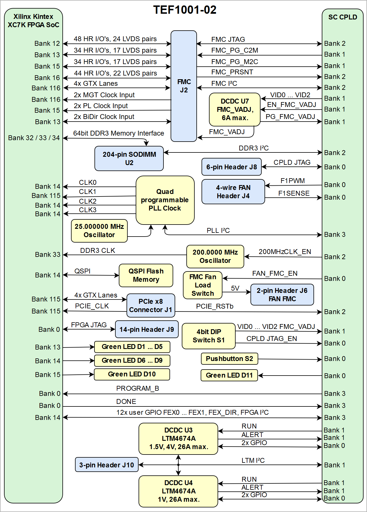
I/O signals and interfaces connected to the FPGA SoCs I/O bank and FMC connector J2:
FPGA Bank
Type
Bank VCCO
12
HR
IO's, 24 LVDS pairs
34 IO's, 17 LVDS pairs
34 IO's, 17 LVDS pairs
44 IO's, 22 LVDS pairs
| FMC |
|---|
| Interfaces | I/O Signal Count |
|---|
| LVDS-pairs count | Connected to | VCCO bank Voltage | Notes |
|---|
J2 |
| I/O | 48 |
| 24 | FPGA Bank 12 HR | FMC_VADJ | Bank voltage FMC_VADJ is supplied by DC-DC converter U7 | |
| 34 | 17 | FPGA Bank 13 |
| HR |
| FMC_VADJ | ||
| 34 | 17 | FPGA Bank 15 |
| HR |
| FMC_VADJ | ||
| 44 | 44 | FPGA Bank 16 |
| HR |
| VIO_B_FMC | Bank voltage VIO_B_FMC is supplied by FMC connector J2 | |
| I²C |
Table 2: General overview of FPGA's PL I/O signals connected to the FMC connector
...
'FMC_SDA', pin C31
'FMC_SCL', pin C30
...
SC CPLD U5, pin 48
SC CPLD U5, pin 49
...
For detailed information about the pin out, please refer to the Pin-out Tables.
| HTML |
|---|
<!--
TO-DO (future):
If Vivado board part files are available for this module, the standard configuration of the MIO pins by using this board part files should be mentioned here. This standard configuration of those pins are also apparent of the on-board peripherals of base-boards related to the module.
--> |
PCI Express Interface
The TEF1001 FPGA board is a PCI Express card designed to fit into systems with PCI Express x8 slots and has a data transmission capability which meets PCIe Gen. 2 with 4 GTX lanes connected to the PCIe interface.
See next section for the overview of FPGA MGT lanes routed to the PCIe interface.
MGT Lanes
| HTML |
|---|
<!--
MGT lanes should be listed separately, as they are more specific than just general I/Os.
--> |
MGT (Multi Gigabit Transceiver) lane consists of one transmit and one receive (TX/RX) differential pairs, two signals each or four signals total per one MGT lane. The MGT lanes are connected to the FMC connector and to the PCIe x8 connector. Following table lists lane number, MGT bank number, transceiver type, signal schematic name, connector and FPGA pins connection:
...
- PER3_P
- PER3_N
- PET3_P
- PET3_N
...
- J1-A29
- J1-A30
- J1-B27
- J1-B28
...
- MGTXTXP0_115, P2
- MGTXTXN0_115, P1
- MGTXRXP0_115, R4
- MGTXRXN0_115, R3
...
- PER2_P
- PER2_N
- PET2_P
- PET2_N
...
- J1-A25
- J1-A26
- J1-B23
- J1-B24
...
- MGTXTXP1_115, M2
- MGTXTXN1_115, M1
- MGTXRXP1_115, N4
- MGTXRXN1_115, N3
...
- PER1_P
- PER1_N
- PET1_P
- PET1_N
...
- J1-A21
- J1-A22
- J1-B19
- J1-B20
...
- MGTXTXP2_115, K2
- MGTXTXN2_115, K1
- MGTXRXP2_115, L4
- MGTXRXN2_115, L3
...
- PER0_P
- PER0_N
- PET0_P
- PET0_N
...
- J1-A16
- J1-A17
- J1-B14
- J1-B15
...
- MGTXTXP3_115, H2
- MGTXTXN3_115, H1
- MGTXRXP3_115, J4
- MGTXRXN3_115, J3
...
- DP3_M2C_P
- DP3_M2C_N
- DP3_C2M_P
- DP3_C2M_N
...
- J2-A10
- J2-A11
- J2-A30
- J2-A31
...
- MGTXRXP0_116, G4
- MGTXRXN0_116, G3
- MGTXTXP0_116, F2
- MGTXTXN0_116, F1
...
- DP2_M2C_P
- DP2_M2C_N
- DP2_C2M_P
- DP2_C2M_N
...
- J2-A6
- J2-A7
- J2-A26
- J2-A27
...
- MGTXRXP1_116, E4
- MGTXRXN1_116, E3
- MGTXTXP1_116, D2
- MGTXTXN1_116, D1
...
- DP1_M2C_P
- DP1_M2C_N
- DP1_C2M_P
- DP1_C2M_N
...
- J2-A2
- J2-A3
- J2-A22
- J2-A23
...
- MGTXRXP2_116, C4
- MGTXRXN2_116, C3
- MGTXTXP2_116, B2
- MGTXTXN2_116, B1
...
- DP0_M2C_P
- DP0_M2C_N
- DP0_C2M_P
- DP0_C2M_N
...
- J2-C6
- J2-C7
- J2-C2
- J2-C3
...
- MGTXRXP3_116, B6
- MGTXRXN3_116, B5
- MGTXTXP3_116, A4
- MGTXTXN3_116, A3
| 2 | - | SC CPLD U5, Bank 2, pin 48, 49 | - | FMC connector J2 is hardware programmed to I²C address 0x50 | |
| JTAG | 5 | - | SC CPLD U5, Bank 2, pin 27, 28, 331, 32 ,36 | 3.3V | - |
| MGT | - | 8 (4 x RX/TX) | Bank 116 GTX | - | 4x MGT lanes |
| Clock Input | - | 2 | Bank 116 GTX | - | 2x Reference clock input to MGT bank |
| Control Signals | 3 | - | SC CPLD U5, Bank 1, pin 68, 69 ,70 | 3.3V | 'FMC_PG_C2M', 'FMC_PG_M2C', 'FMC_PRSNT_M2C_L' |
Table 2: FMC connector J2 interface
For detailed information about the pin out, please refer to the Pin-out Tables.
FMC connector J2 MGT Lanes:
| FMC | MGT Lane | Bank | Type | Signal Schematic Name | FMC Connector Pin | FPGA Pin |
|---|---|---|---|---|---|---|
J2 | 0 | 116 | GTX |
|
|
|
| 1 | 116 | GTX |
|
|
| |
| 2 | 116 | GTX |
|
|
| |
| 3 | 116 | GTX |
|
|
|
Table 3: FMC connector J2 MGT lanes
FMC connector J2 reference clock sources:
| FMC | Signal Schematic Name | Connected to | FMC Connector Pin | FPGA Pin | Notes |
|---|---|---|---|---|---|
J2 |
| MGT bank 116 | J2-D4 | MGTREFCLK0P_116, D6 | Supplied by attached FMC module |
| MGT bank 116 | J2-B20 J2-B21 | MGTREFCLK1P_116, F6 MGTREFCLK1N_116, F5 | Supplied by attached FMC module |
Table 4: FMC connector J2 clock signal input
FMC connector J2 VCC/VCCIO:
| FMC | Available VCC/VCCIO | FMC Connector Pin | Source | Notes |
|---|---|---|---|---|
J2 | 3V3FMC | J2-D36 | DCDC U15, | Enable by SC CPLD U5, bank 1, pin 60 |
| 3V3 | J2-D32 | LDO U9, max. current: 0.5A | not dedicated for FMC connector | |
| 12V | J2-C35 | external source through | - | |
| FMC_VADJ | J2-H40 | DCDC U7, | Enable by SC CPLD U5, bank 1, pin 51 |
Table 5: FMC connector J2 available VCC/VCCIO
FMC connector J2 Cooling Fan:
| FMC | Fan Designator | Enable Signal | Notes |
|---|---|---|---|
J2 | M1 | Enable by SC CPLD U5, bank 0, pin 78 | - |
Table 6: FMC connector J2 cooling fan
| HTML |
|---|
<!--
TO-DO (future):
If Vivado board part files are available for this module, the standard configuration of the MIO pins by using this board part files should be mentioned here. This standard configuration of those pins are also apparent of the on-board peripherals of base-boards related to the module.
--> |
PCI Express Interface
The TEF1001 FPGA board is a PCI Express card designed to fit into systems with PCI Express x8 slots and has a data transmission capability which meets PCIe Gen. 2 with 4 GTX lanes routed to the PCIe interface.
Following table lists lane number, MGT bank number, transceiver type, signal schematic name, connector and FPGA pins connection:
| Lane | Bank | Type | Signal Name | PCIe Connector Pin | FPGA Pin |
|---|---|---|---|---|---|
| 0 | 115 | GTX |
|
|
|
| 1 | 115 | GTX |
|
|
|
| 2 | 115 | GTX |
|
|
|
| 3 | 115 | GTX |
|
|
|
Table 7: GTX lanes routed to the PCIe interface
| PCIe | Signal Schematic Name | Connected to | PCIe connector pin | FPGA Pin | Notes |
|---|---|---|---|---|---|
J1 |
| MGT bank 115 | J1-A13, REFCLK+ | MGTREFCLK1P_115, K6 | External clock supplied by PCIe interface |
Table 8: PCIe reference clock sources
JTAG Connectors
There are two JTAG connectors J8 and J9
...
Below are listed MGT banks reference clock sources:
...
Table 4: MGT reference clock sources
JTAG Interface
There are three JTAG interfaces available on the TEF1001 board:
| JTAG Interface | Signal Schematic Name | JTAG Connector Pin | Connected to | |||
|---|---|---|---|---|---|---|
CPLD JTAG VCCIO: 3.3V Connector: J8 | CPLD_JTAG_TMS | J8-1 | SC CPLD, bank 0, pin 90 | |||
| CPLD_JTAG_TDI | J8-2 | SC CPLD, bank 0, pin 94 | ||||
| CPLD_JTAG_TDO | J8-3 | SC CPLD, bank 0, pin 95 | ||||
| CPLD_JTAG_TCK | J8-4 | SC CPLD, bank 0, pin 91 | ||||
FPGA JTAG VCCIO: 1.8V Connector: J9 | FPGA_JTAG_TMS | J9-4 | FPGA, bank 0, pin N9 | |||
| FPGA_JTAG_TCK | J9-6 | FPGA, bank 0, pin M8 | ||||
| FPGA_JTAG_TDO | J9-8 | FPGA, bank 0, pin N8 | ||||
-4 | SC CPLD | FPGA_JTAG_TDI | J9-10 | FPGA, bank 0, pin L891 | FMC||
FPGA JTAG VCCIO: | 31. | 3V8V Connector: | J2J9 | FMCFPGA_JTAG_TRSTTMS | J2J9-D344 | SC CPLDFPGA, bank 20, pin 36N9 |
| FMCFPGA_JTAG_TCK | J2J9-D296 | SC CPLDFPGA, bank 20, pin 27M8 | ||||
| FMCFPGA_JTAG_TMSTDO | J2J9-D338 | SC CPLDFPGA, bank 20, pin 28N8 | ||||
| FMCFPGA_JTAG_TDI | J2J9-D3010 | SC CPLDFPGA, bank 20, pin 31 | FMC_TDO | J2-D31 | SC CPLD, bank 2, pin 32L8 |
Table 5: JTAG interface signals
...
For detailed information, refer to the reference page of the SC CPLD firmware of this module. Table below lists the SC CPLD I/O pins with their default configuration:
| Pin Name | SC CPLD Direction | Function | Default Configuration |
|---|---|---|---|
| 200MHZCLK_EN | out | control line | enables 200.0000MHz oscillator U1 |
| BUTTON | in | user | Reset Button |
| CPLD_TDO | out | CPLD JTAG interface | - |
| CPLD_TDI | in | ||
| CPLD_TCK | in | ||
| CPLD_TMS | in | ||
| JTAG_EN | in | ||
| DDR3_SCL | in / out | I²C bus of DDR3 SODIMM socket | I²C connected to FPGA |
| DDR3_SDA | in / out | ||
| PLL_SCL | in / out | I²C bus of SI5338 quad clock PLL | I²C connected to FPGA |
| PLL_SDA | in / out | ||
| PCIE_RSTB | in | PCIe reset input | see current SC CPLD firmware |
| FEX_DIR / FEX0 ... FEX11 | in / out | user GPIO | see current SC CPLD firmware |
| F1PWM | out | FPGA FAN control | see current SC CPLD firmware |
| F1SENSE | in | ||
| FAN_FMC_EN | out | FMC FAN enable | |
| FMC_PG_C2M | out | FMC signals and pins | see current SC CPLD firmware |
| FMC_PG_M2C | in | ||
| FMC_PRSNT_M2C_L | in | ||
| FMC_SCL | in / out | FMC I²C | I²C connected to FPGA |
| FMC_SDA | in / out | ||
| FMC_TCK | FMC JTAG | see current SC CPLD firmware | |
| FMC_TDI | |||
| FMC_TDO | |||
| FMC_TMS | |||
| FMC_TRST | |||
| DONE | in | FPGA configuration signal | PL configuration completed |
| PROGRAM_B | out | PL configuration reset signal | |
| LED1 | out | LED status signal | see current CPLD firmware |
| FPGA_IIC_OE | in | SC CPLD works as I²C switch with the FPGA as I²C-Master and on-board peripherals as I²C-slaves | I²C output enable, connected to PL bank 14 pin F25 |
| FPGA_IIC_SCL | in / out | I²C clock line, connected to PL bank 14 pin G26 | |
| FPGA_IIC_SDA | in / out | I²C data line, connected to PL bank 14 pin G25 | |
| EN_1V8 | out | Power control | enable signal DCDC U20 '1V8' |
| PG_1V8 | in | power good signal DCDC U20 '1V8' | |
| EN_3V3FMC | out | enable signal DCDC U15 'EN_3V3FMC' | |
| PG_3V3 | in | power good signal U15 'EN_3V3FMC' | |
| EN_FMC_VADJ | out | enable signal DCDC U7 'FMC_VADJ' | |
| PG_FMC_VADJ | in | power good DCDC U7 'FMC_VADJ' | |
VID0_FMC_VADJ, | out | DCDC U7 power selection pin | |
VID0_FMC_VADJ_CTRL, | in | Power selection of FMC_VADJ, forwarded to DCDC U7 | |
| LTM_1V5_RUN | out | enable signals of DCDC U3, U4 (LTM4676) see current CPLD firmware | |
| LTM_4V_RUN | out | ||
| LTM_SCL | in / out | DCDC U3, U4 (LTM4676) I²C | I²C connected to FPGA |
| LTM_SDA | in / out | ||
| LTM1_ALERT | in | DCDC U3, U4 (LTM4676) control | see current CPLD firmware |
| LTM2_ALERT | in | ||
| LTM_1V_IO0 | in / out | ||
| LTM_1V_IO1 | in / out | ||
| LTM_1V5_4V_IO0 | in / out | ||
| LTM_1V5_4V_IO1 | in / out |
Table 6: System Controller CPLD I/O pins
...
There is also a I2C interface between the System Controller CPLD U5 and the DDR3 SODIMM memory socket U2.
| I²C Interface | Schematic net names | Connected to | I²C Address | Notes |
|---|---|---|---|---|
| DDR3 SODIMM, U2 | 'DDR3_SDA', pin 200 | SC CPLD U5, pin 42 | module dependent | - |
Table 8: DDR3 SODIMM socket I²C interface
...
Quad SPI Flash memory interface is connected to the FPGA bank 14, QSPI clock is provided by FPGA config bank 0.
| Signal Name | QSPI Flash Memory U12 Pin | FPGA Pin |
|---|---|---|
| FLASH_QSPI_CS | S, Pin 7 | Bank 14, Pin C23 |
| FLASH_QSPI_D00 | DQ0, Pin 15 | Bank 14, Pin B24 |
| FLASH_QSPI_D01 | DQ1, Pin 8 | Bank 14, Pin A25 |
| FLASH_QSPI_D02 | DQ2, Pin 9 | Bank 14, Pin B22 |
| FLASH_QSPI_D03 | DQ3, Pin 1 | Bank 14, Pin A22 |
| FPGA_CFG_CCLK | C, Pin 16 | Bank 0, Pin C8 |
Table 7: Quad SPI interface signals and connections
...
On-board DC-DC converters U3 (1V5 and 4V) and U4 (1V) are provided by Linear Technology LTM4676 with special I/O's and I²C interface:
| LTM4676 U3 pin | Schematic net names | Connected to | Notes |
|---|---|---|---|
| SDA, pin D6 SCL, pin E6 | 'LTM_SDA' | SC CPLD U5, pin 66 | I²C Address: 0x40 I²C interface of LTM4676 |
| ALERT, pin E5 | 'LTM2_ALERT' | SC CPLD U5, pin 64 | active low |
| GPIO0, pin E4 | 'LTM_1V5_4V_IO0' | SC CPLD U5, pin 85 | active low |
| GPIO1, pin F4 | 'LTM_1V5_4V_IO1' | SC CPLD U5, pin 83 | active low |
| LTM4676 U4 pin | Schematic net names | Connected to | Notes |
SDA, pin D6 | 'LTM_SDA' | SC CPLD U5, pin 66 | I²C Address: 0x4F I²C interface of LTM4676 |
| ALERT, pin E5 | 'LTM1_ALERT' | SC CPLD U5, pin 65 | active low |
| GPIO0, pin E4 | 'LTM_1V_IO0' | SC CPLD U5, pin 86 | active low |
| GPIO1, pin F4 | 'LTM_1V_IO1' | SC CPLD U5, pin 88 | active low |
Table 8: DCDC converters U3 and U4 I/O's and interfaces
...
Overview
Content Tools