...
...
| Scroll Title |
|---|
| anchor | Figure_OV_BD |
|---|
| title | TEI0006 block diagram |
|---|
|
| Scroll Ignore |
|---|
| draw.io Diagram |
|---|
| border | false |
|---|
| viewerToolbar | true |
|---|
| |
|---|
| fitWindow | false |
|---|
| diagramDisplayName | |
|---|
| lbox | false |
|---|
| revision | 24 |
|---|
| diagramName | TEI0006_OV_BD |
|---|
| simpleViewer | false |
|---|
| width | |
|---|
| links | auto |
|---|
| tbstyle | hidden |
|---|
| lbox | true |
|---|
| diagramWidth | 632 | revision | 22639 |
|---|
|
|
| Scroll Only |
|---|
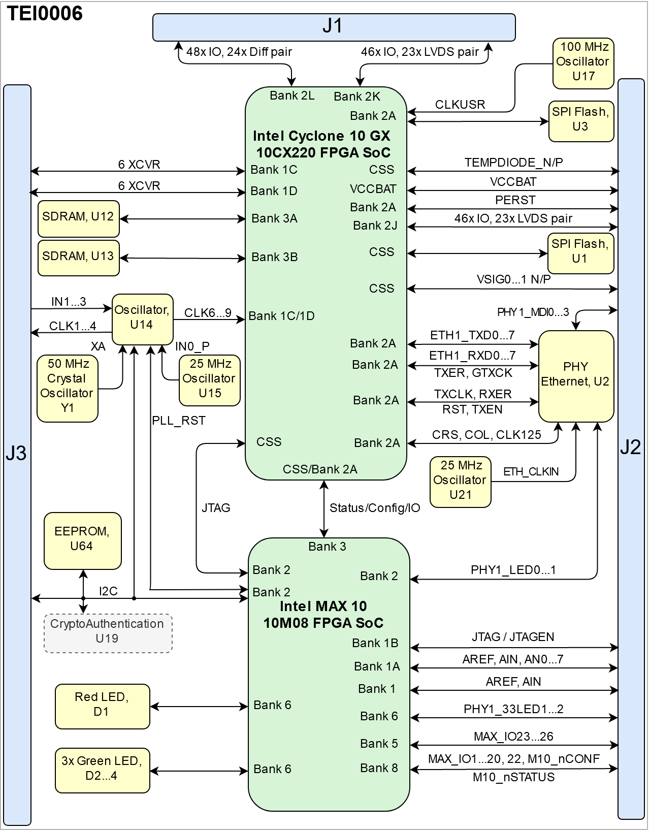 Image Modified Image Modified
|
|
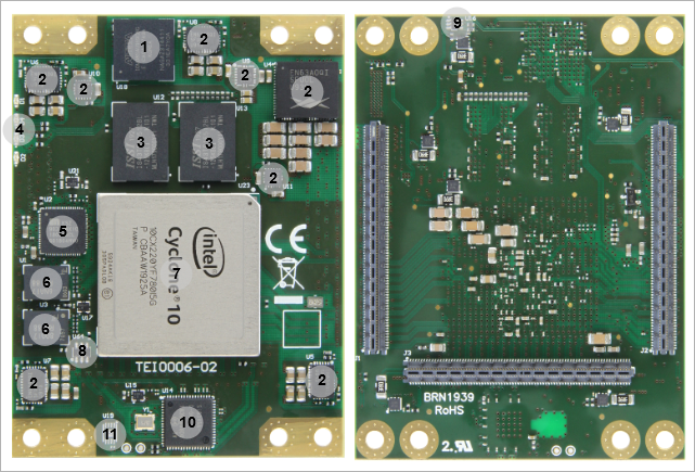
Main Components
...
| Scroll Title |
|---|
| anchor | Figure_OV_BD |
|---|
| title | TEI0006 main components |
|---|
|
| Scroll Ignore |
|---|
| draw.io Diagram |
|---|
| border | false |
|---|
| viewerToolbar | true |
|---|
| |
|---|
| fitWindow | false |
|---|
| diagramDisplayName | |
|---|
| lbox | false |
|---|
| revision | 8 |
|---|
| diagramName | TEI0006_OV_MC |
|---|
| simpleViewer | false |
|---|
| width | |
|---|
| links | auto |
|---|
| tbstyle | hidden |
|---|
| lbox | true |
|---|
| diagramWidth | 641 | revision | 6 |
|---|
|
|
| Scroll Only |
|---|
|
|
- Intel® MAX 10, U18
- DC/DC convertor, U4...11
- SDRAM DDR3 Memory, U12 - U13
- User LEDs, D1...4
- Ethernet Transceiver, U2
- SPI Flash Memory, U1 - U3
- Intel® Cyclone 10 GX, U23
- EEPROM, U64
- Buffer, U16
- 10-Channel Clock Multiplier, U14
- CryptoAuthentication Device (optional), U19
Initial Delivery State
| Page properties |
|---|
|
Notes : Only components like EEPROM, QSPI flash and DDR3 can be initialized by default at manufacture. If there is no components which might have initial data ( possible on carrier) you must keep the table empty |
...
| Scroll Title |
|---|
| anchor | Table_OV_IDS |
|---|
| title | Initial delivery state of programmable devices on the module |
|---|
|
| Scroll Table Layout |
|---|
| orientation | portrait |
|---|
| sortDirection | ASC |
|---|
| repeatTableHeaders | default |
|---|
| sortByColumn | 1 |
|---|
| sortEnabled | false |
|---|
| cellHighlighting | true |
|---|
|
Storage device name | Content | Notes |
|---|
| Intel® MAX 10 | Programmed | See CPLD Firmware | Quad SPI Flash | Not Programmed |
| | EEPROM | Quad SPI Flash | Not Programmed | EEPROM | Programmed | Ethernet MAC | | DDR3 SDRAM | Not Programmed |
|
|
...
| Scroll Title |
|---|
| anchor | Table_SIP_B2B |
|---|
| title | General PL I/O to B2B connectors information |
|---|
|
| Scroll Table Layout |
|---|
| orientation | portrait |
|---|
| sortDirection | ASC |
|---|
| repeatTableHeaders | default |
|---|
| sortByColumn | 1 |
|---|
| sortEnabled | false |
|---|
| cellHighlighting | true |
|---|
|
| FPGA | FPGA Bank | B2B Connector | I/O Signal Count | Voltage Level | Notes |
|---|
Intel Cyclone 10 GX | Bank 1C | J3 | 24 Single ended (12 Diff pair) | 0.95V | GXBL1C_RX0...5 N/P, GXBL1C_TX0...5 N/P | Bank 1D | J3 | 24 Single ended (12 Diff pair) | 0.95V | GXBL1D_RX0...5 N/P, GXBL1D_TX0...5 N/P | Bank 2A | J2 | 2 Single ended | 1.8V | PERST, CLKUSR | Bank 2J | J2 | 46 Single ended (23 Diff pair) | VCCIO2J |
| Bank 2K | J1 | 46 Single ended (23 Diff pair) | VCCIO2K |
| Bank 2L | J1 | 48 Single ended (24 Diff pair) | VADJ up to 3 V |
| Bank 3A | - | - | 1.35V | VDD_DDR | Bank 3B | - | - | 1.35V | VDD_DDR | Intel Max 10 | Bank 1A | J2 | 8 Single ended | 3.3V |
| Bank 1B | J2 | 5 Single ended | 3.3V |
| Bank 2 | J3 | 2 1 Single ended | 1.8VIO |
| Bank 3 | - | - | 1.8VIO |
| Bank 5 | J2 | 4 3 Single ended | 3.3V |
| Bank 6 | J2 | 2 Single ended | 3.3V |
| Bank 8 | J2 | 24 23 Single ended | 3.3V |
|
|
JTAG Interface
JTAG access to the TEI0006 SoM is through B2B connector J2. JTAGEN is pulled up to 3.3V and after power on, JTAG will be enabledfor MAX 10 CPLD is enabled. JTAG port of Cyclon 10 GX device is routed to MAX10 CPLD IOs. The default Firmware connects the JTAG port of the Cyclon 10 GX to the IO pins of the JTAG port in user IO mode. Setting JTAGEN to GND enables JTAG for the Cyclon 10 GX device.
| Scroll Title |
|---|
| anchor | Table_SIP_JTG |
|---|
| title | JTAG pins connection |
|---|
|
| Scroll Table Layout |
|---|
| orientation | portrait |
|---|
| sortDirection | ASC |
|---|
| repeatTableHeaders | default |
|---|
| sortByColumn | 1 |
|---|
| sortEnabled | false |
|---|
| cellHighlighting | true |
|---|
|
JTAG Signal | B2B Connector | Note |
|---|
| TMS | J2-160 |
| | TDI | J2-159 |
| | TDO | J2-158 |
| | TCK | J2-157 |
| | JTAGEN | J2-105 | Pulled up to 3.3V. |
|
...
| Page properties |
|---|
|
you must fill the table below with group of MIOs which are connected to a specific components or peripherals, you do not have to specify pins in B2B, Just mention which B2B is connected to MIOs. The rest is clear in the Schematic. Example: | MIO Pin | Connected to | B2B | Notes |
|---|
| MIO12...14 | SPI_CS , SPI_DQ0... SPI_DQ3 SPI_SCK | J2 | QSPI |
|
| Scroll Title |
|---|
| anchor | Table_OBP_MIOs |
|---|
| title | MIOs pins |
|---|
|
| Scroll Table Layout |
|---|
| orientation | portrait |
|---|
| sortDirection | ASC |
|---|
| repeatTableHeaders | default |
|---|
| sortByColumn | 1 |
|---|
| sortEnabled | false |
|---|
| cellHighlighting | true |
|---|
|
| MIO Pin | Connected to | B2B | Notes |
|---|
| MAX_IO1...20, 22 | U18 (Intel MAX 10) - Bank 8 | J2 |
| | MAX_IO23..., 25, 26 | U18 (Intel MAX 10) - Bank 5
| J2 |
|
|
...
| Scroll Title |
|---|
| anchor | Table_OBP |
|---|
| title | On board peripherals |
|---|
|
| Scroll Table Layout |
|---|
| orientation | portrait |
|---|
| sortDirection | ASC |
|---|
| repeatTableHeaders | default |
|---|
| sortByColumn | 1 |
|---|
| sortEnabled | false |
|---|
| cellHighlighting | true |
|---|
|
|
QSPI Flash Memory
| Page properties |
|---|
|
Notes : Minimum and Maximum density of quad SPI flash must be mentioned for other assembly options. |
...
Clock Sources
The TEI0006 has three crystal oscillator one crystal, three MEMS oscillators and a programmable clock generator.
| Scroll Title |
|---|
| anchor | Table_OBP_CLK |
|---|
| title | Osillators |
|---|
|
| Scroll Table Layout |
|---|
| orientation | portrait |
|---|
| sortDirection | ASC |
|---|
| repeatTableHeaders | default |
|---|
| sortByColumn | 1 |
|---|
| sortEnabled | false |
|---|
| cellHighlighting | true |
|---|
|
| Designator | Description | Frequency |
|---|
NoteCrystal | MEMS Oscillator | 25MHz | U2 Ethernet | | U15 |
Crystal | MEMS Oscillator | 25MHz | IN0 of U14 | | U17 | MEMS Oscillator | 100 MHz | U23, BANK2A USRCLK | | Y1 | Crystal Oscillator |
48MHz| 50MHz | crystal input of U14 | | U14 | Programmable Oscillator | Variable | - |
|
| Scroll Title |
|---|
| anchor | Table_OBP_CLK_PO |
|---|
| title | Programmable Oscillator connections |
|---|
|
| Scroll Table Layout |
|---|
| orientation | portrait |
|---|
| sortDirection | ASC |
|---|
| repeatTableHeaders | default |
|---|
| sortByColumn | 1 |
|---|
| sortEnabled | false |
|---|
| cellHighlighting | true |
|---|
|
| Signals | Clock Type | In/ Out | Connected to | Frequency | Note |
|---|
IN0_P IN0_N | Differential | In In | Oscillator, U15 GND | 25 MHz |
| | IN1..3 IN3 | Differential | In | B2B, J3 | Variable |
| XA, XB | Differential |
| Oscillator, U17Y1 GND | 48 50 MHz |
| CLK0 | Differential | Out | Intel Cyclon Cyclone 10 GX (U23)- Bank 2A | User | Default off | CLK1...4 | Differential | Out | B2B, J3 | User | Default off | | REFCLK_EMIFP | Differential | Out | Intel Cyclon 10 GX (U23)- Bank 3B | User | Default off | | CLK6...7 | Differential | Out | Intel Cyclon 10 GX (U23)- Bank 1D | User | Default off | | CLK8...9 | Differential | Out | Intel Cyclon 10 GX (U23)- Bank 1C | User | Default off |
|
Power and Power-On Sequence
CryptoAuthentication
ATECC608A (U19) is a CryptoAuthentication device connected to the I2C bus. This chip is optional, for further description see datasheet of manufacturer.
| Scroll Title |
|---|
| anchor | Table_OBP_EEP |
|---|
| title | I2C Interface of CryptoAuthentication |
|---|
|
| Scroll Table Layout |
|---|
| orientation | portrait |
|---|
| sortDirection | ASC |
|---|
| repeatTableHeaders | default |
|---|
| sortByColumn | 1 |
|---|
| sortEnabled | false |
|---|
| cellHighlighting | true |
|---|
|
| Schematic | U19 Pin | B2B | U18 Intel Max 10 Pin | Notes |
|---|
| I2C_SCL | SCL | J3-135 | Bank 2 - K2 | - | | I2C_SDA | SDA | J3-137 | Bank 2 - L2 | - |
|
Power and Power-On Sequence
| Page properties |
|---|
|
| Page properties |
|---|
|
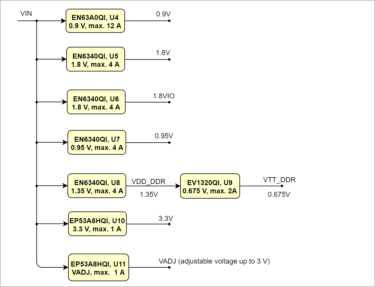
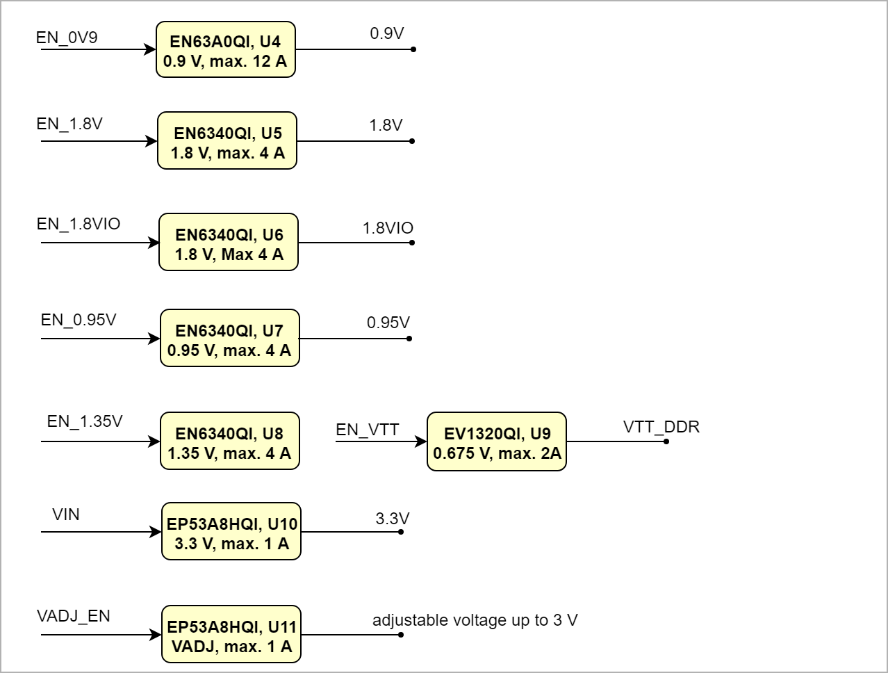
In 'Power and Power-on Sequence' section there are three important digrams which must be drawn: - Power on-sequence
- Power distribution
- Voltage monitoring circuit
|
...
| Scroll Title |
|---|
| anchor | Figure_PWR_PD |
|---|
| title | Power Distribution |
|---|
|
| Scroll Ignore |
|---|
| draw.io Diagram |
|---|
| border | false |
|---|
| viewerToolbar | true |
|---|
| |
|---|
| fitWindow | false |
|---|
| diagramDisplayName | |
|---|
| lbox | truefalse |
|---|
| revision | 1011 |
|---|
| diagramName | TEI0006_PWR_PD |
|---|
| simpleViewer | false |
|---|
| width | |
|---|
| links | auto |
|---|
| tbstyle | hidden |
|---|
| diagramWidth | 482639 |
|---|
|
|
| Scroll Only |
|---|
|
|
Power-On Sequence
...
| Scroll Title |
|---|
| anchor | Figure_PWR_PS |
|---|
| title | Power Sequence |
|---|
|
| Scroll Ignore |
|---|
| draw.io Diagram |
|---|
| border | false |
|---|
| viewerToolbar | true |
|---|
| |
|---|
| fitWindow | false |
|---|
| diagramDisplayName | |
|---|
| lbox | truefalse |
|---|
| revision | 89 |
|---|
| diagramName | TEI0006_PWR_PS |
|---|
| simpleViewer | false |
|---|
| width | |
|---|
| links | auto |
|---|
| tbstyle | hidden |
|---|
| diagramWidth | 482639 |
|---|
|
|
| Scroll Only |
|---|
|
|
Power Rails
| Scroll Title |
|---|
| anchor | Table_PWR_PR |
|---|
| title | Module power rails. |
|---|
|
| Scroll Table Layout |
|---|
| orientation | portrait |
|---|
| sortDirection | ASC |
|---|
| repeatTableHeaders | default |
|---|
| sortByColumn | 1 |
|---|
| sortEnabled | false |
|---|
| cellHighlighting | true |
|---|
|
| Power Rail Name | B2B Connector J1 Pin | B2B Connector J2 Pin | B2B Connector J3 Pin | Voltage Level | Direction | Notes |
|---|
| VIN | 145, 147,149, 151, 153, 155, 157, 159 | - | - | 5 V | Input |
| | VCCIO2K | 53, 54 | - | - | 1.2 V, 1.25 V, 1.35 |
V, 1.5 V, 1.8 2 30 | 8 V | Input |
| | VADJ | 140,142 | - | - | adjustable between 1.8 V - 3.0 V | Output | Voltages according to EP53A8HQI datasheet but restricted to allowed bank voltage | | VCCIO2J | - | 29,30 | - | 1.2 V, 1.25 V, 1.35 V, 1.5 V |
, V, 2.5 or 3.0 V | Input |
| 3.3V | - | 149,150 | - | 3.3 V | Output |
| | 1.8_VIO | - | - | 139 | 1.8 V | Output |
|
|
Bank Voltages
| Scroll Title |
|---|
| anchor | Table_PWR_BV |
|---|
| title | SoC bank voltages. |
|---|
|
| Scroll Table Layout |
|---|
| orientation | portrait |
|---|
| sortDirection | ASC |
|---|
| repeatTableHeaders | default |
|---|
| sortByColumn | 1 |
|---|
| sortEnabled | false |
|---|
| cellHighlighting | true |
|---|
|
| FPGA | FPGA Bank | Voltage Level | Notes |
|---|
| Intel Cyclone 10 GX | Bank 1C | 0.95 V |
| Bank 1D | 0.95 V |
| | Bank 2A | 1.8 V | 1.8VIO | | Bank 2J | 1.2 V, 1.25 V, 1.35 V, 1.5 V , or 1.8 V, 2.5 V or 3.0 V | VCCIO2J | | Bank 2K | 1.2 V, 1.25 V, 1.35 V, 1.5 V , or 1.8 V, 2.5 V or 3.0 V | VCCIO2K | | Bank 2L | adjustable between 1.8 V - 3.0 V | Voltages according to EP53A8HQI datasheet | | Bank 3A | 1.35 V | VDD_DDR | | Bank 3B | 1.35 V | VDD_DDR | | Intel Max 10 | Bank 1A | 3.3 V |
| | Bank 1B | 3.3 V |
| | Bank 2 | 1.8 V | 1.8VIO | | Bank 3 | 1.8 V | 1.8VIO | | Bank 5 | 3.3V |
| | Bank 6 | 3.3V |
| | Bank 8 | 3.3V |
|
|
...
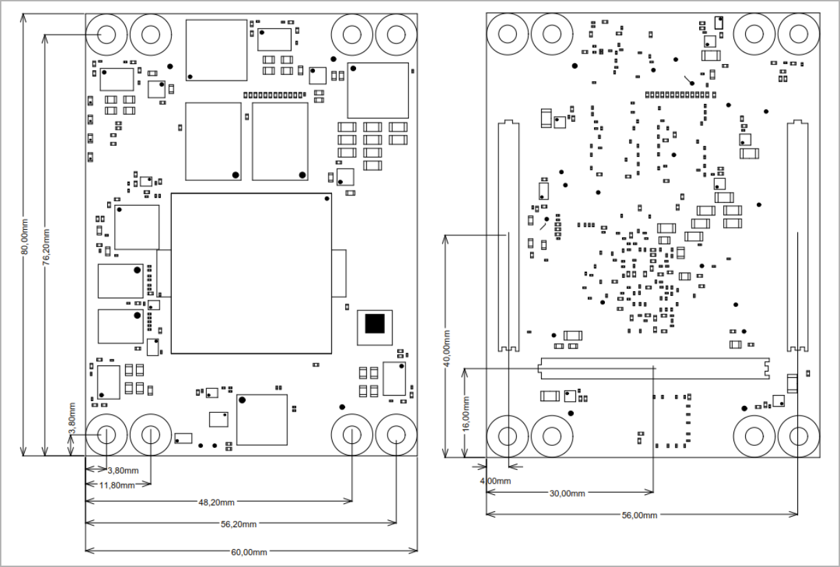
| Scroll Title |
|---|
| anchor | Figure_TS_PD |
|---|
| title | Physical Dimension |
|---|
|
| Scroll Ignore |
|---|
| draw.io Diagram |
|---|
| border | false |
|---|
| viewerToolbar | true |
|---|
| |
|---|
| fitWindow | false |
|---|
| diagramDisplayName | |
|---|
| lbox | truefalse |
|---|
| revision | 23 |
|---|
| diagramName | TEI0006_TS_PD |
|---|
| simpleViewer | false |
|---|
| width | |
|---|
| links | auto |
|---|
| tbstyle | hidden |
|---|
| diagramWidth | 641611 |
|---|
|
|
| Scroll Only |
|---|
| scroll-pdf | true |
|---|
| scroll-office | true |
|---|
| scroll-chm | true |
|---|
| scroll-docbook | true |
|---|
| scroll-eclipsehelp | true |
|---|
| scroll-epub | true |
|---|
| scroll-html | true |
|---|
| 
|
|
...
| Scroll Title |
|---|
| anchor | Table_RH_HRH |
|---|
| title | Hardware Revision History |
|---|
|
| Scroll Table Layout |
|---|
| orientation | portrait |
|---|
| sortDirection | ASC |
|---|
| repeatTableHeaders | default |
|---|
| sortByColumn | 1 |
|---|
| sortEnabled | false |
|---|
| cellHighlighting | true |
|---|
| default |
|---|
| sortByColumn | 1 |
|---|
| sortEnabled | false |
|---|
| cellHighlighting | true |
|---|
|
| Date | Revision | Changes | Documentation Link |
|---|
| 202-12-23 | 03 | - two input cloock signals on B2B connected directly to GXBL1C bank
| REV03 | | 2019-09-11 | 02 | - added 100MHz MEMS oscillator, remove CLKUSR signal from J2
- replaced U21/U15 by SiT8008
- added pull-up to M10_NSTATUS signal
- added pull-up to M10_DEVCLRN, removed signal from J2
- added optional CryptoAuthentication chip U19
| REV02 | | Date | Revision | Changes | Documentation Link |
|---|
| 2018-08-10 | 01 | - | REV01 |
|
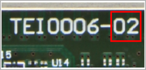
Hardware revision number can be found on the PCB board together with the module model number separated by the dash.
| Scroll Title |
|---|
| anchor | Figure_RV_HRN |
|---|
| title | Board hardware revision number. |
|---|
|
| Scroll Ignore |
|---|
| draw.io Diagram |
|---|
| border | truefalse |
|---|
| viewerToolbar | true |
|---|
| |
|---|
| fitWindow | false |
|---|
| diagramDisplayName | |
|---|
| lbox | false |
|---|
| revision | 3 |
|---|
| diagramName | TEI0006_RV_RHN |
|---|
| simpleViewer | false |
|---|
| width | |
|---|
| links | auto |
|---|
| diagramWidthtbstyle | 197top |
|---|
| revisiondiagramWidth | 1178 |
|---|
|
|
| Scroll Only |
|---|
| scroll-pdf | true |
|---|
| scroll-office | true |
|---|
| scroll-chm | true |
|---|
| scroll-docbook | true |
|---|
| scroll-eclipsehelp | true |
|---|
| scroll-epub | true |
|---|
| scroll-html | true |
|---|
| 
|
|
...
| Scroll Title |
|---|
| anchor | Table_RH_DCH |
|---|
| title | Document change history. |
|---|
|
| Scroll Table Layout |
|---|
| orientation | portrait |
|---|
| sortDirection | ASC |
|---|
| repeatTableHeaders | default |
|---|
| sortByColumn | 1 |
|---|
| sortEnabled | false |
|---|
| cellHighlighting | true |
|---|
|
| Date | Revision | Contributor | Description |
|---|
| Page info |
|---|
| infoType | Modified date |
|---|
| dateFormat | yyyy-MM-dd |
|---|
| type | Flat |
|---|
|
| | Page info |
|---|
| infoType | Current version |
|---|
| prefix | v. |
|---|
| type | Flat |
|---|
| showVersions | false |
|---|
|
| | Page info |
|---|
| infoType | Modified by |
|---|
| type | Flat |
|---|
| showVersions | false |
|---|
|
| - corrected Bank Voltages for Bank 2J (VCCIO2J) and Bank 2K (VCCIO2K)
| | 2022-03-18 | v.85 | Vitali Tsiukala | - Added Info about Gigabit Transceivers
| | 2021-06-07 | | Martin Rohrmüller | - corrected Physical Dimension figure
- updated to REV03
| | v.82 | Martin Rohrmüller | | 2019-06-14 | v.80 | Pedram Babakhani | Figures updated - Technical specifications updated
| | v.69 | Pedram Babakhani | | -- | all | | Page info |
|---|
| infoType | Modified users |
|---|
| type | Flat |
|---|
| showVersions | false |
|---|
|
| |
|
...