...
The Trenz Electronic TEF1002-02 ... is an industrial-grade ... module ... based on Xilinx ...carrier is a baseboard for Trenz Electronic 4 x 5 SoMs. It is a PCIe x1 card and also hosts and LPC FMC connector.
See page "4 x 5 cm carriers" to get information about the SoMs supported by the TEF1002 carrier board.
Refer to trenz.org/tef1002-info for Refer to http://trenz.org/tec0850-info for the current online version of this manual and other available documentation.
...
- ANSI/VITA 57.1 compliant FMC LPC connector, J1
- Cooling fan 5VDC M1 (45X5MM, 0.7W, 1.06CFM), M1
- SFP+ connector, J12
- PCIe x1 connector, J3
- SATA connector with pin 7 power configuration, J31
- Trenz Electronic 4 x 5 modules B2B connectors, JB1 ... JB3
- RJ45 Gigabit Ethernet connector, J9
- 2x high speed LVDS arrangement of connectors J11, J13, J14, J18
- Micro-USB2 connector, J10
- FTDI FT2232H USB2 to JTAG,UART/FIFO Bridge, U4
- Micro-USB2 connector, J16
- MAX10 10M08SAU169C8G CPLD, U11
- 6-pin 12V power connector, J15
- 5x2 CPLD JTAG pin header for TEI0004, J5
- 3x1 jumper pin header (select VCCIOA), J4
- 3x1 jumper pin header (select VCCA_SD), J7
- 3x1 pin header (VBAT), J6
- 2x3 pin header (MIO/PJTAG), J19
- Push button, S1
- 10x dip switch, S2, S3
- DCDC LTM4638 @5.0V, U9
- DCDC EN6338QI @3.3V, U10
- 2x green LED (user), D1, D2
- green LED (Power), D3
- green LED (Status), D4
- SD-Card connector (top loader),
- DCDC EN5335QI (FMC_VADJ), U1
- DCDC EN6338QI @3.3V (3V3FMC), U14
- SDIO Level shifter TXS02612, U3
...
| Scroll Title |
|---|
| anchor | Table_SIP_PCIe |
|---|
| title | PCIe x1 card edge connector |
|---|
|
| Scroll Table Layout |
|---|
| orientation | portrait |
|---|
| sortDirection | ASC |
|---|
| repeatTableHeaders | default |
|---|
| sortByColumn | 1 |
|---|
| sortEnabled | false |
|---|
| cellHighlighting | true |
|---|
|
| Connector J3 Pins and Interfaces | I/O Signal Count | diff.-pairs count | Connected to | VCCIO voltage | Notes |
|---|
| Multi Gigabit Transceiver | - | 2 | B2B JB3 connector, pin 25, 27 and 26, 28 | - | RX, TX | | Clock | - | 1 | B2B JB3 connector, pin 32, 34 | - |
| | JTAG | 5 | - | SC CPLD U11, M12, M13, L11, N12, G10 | 3V3IN | TDO, TMS, TCK, TDI, TRST |
|
SATA connector
The SATA connector includes the pin 7 power configuration. This means that pin 7 (usually GND) is connected to a power switch U15, applying 5V to this pin. This gives the possibility to use SATADoMs with pin 7 power configuration. If a standard SATA device is connected the short (Current >0.5A) of Pin7 to GND is detected by the powerswitch and the powerswitch is switched OFF by the CPLD until a powercycle of TEF1002. There is also the possibility to remove the pin 7 power configuration by removing R82 and assembling R83 (0 Ohm, 2012 (0805)).
| Scroll Title |
|---|
| anchor | Table_SIP_SATA |
|---|
| title | SATA connector |
|---|
|
|
| Scroll Title |
|---|
| anchor | Table_SIP_SATA |
|---|
| title | SATA connector |
|---|
|
| Scroll Table Layout |
|---|
| orientation | portrait |
|---|
| sortDirection | ASC |
|---|
| repeatTableHeaders | default |
|---|
| sortByColumn | 1 |
|---|
| sortEnabled | false |
|---|
| cellHighlighting | true |
|---|
|
| Connector J31 Pins and Interfaces | I/O Signal Count | diff.-pairs count | Connected to | VCCIO voltage | Notes |
|---|
| Multi Gigabit Transceiver, pin 5,6 and 2,3 | - | 2 | B2B JB3 connector, pin 7, 9 and 8, 10 | - | RX, TX | - | RX, TX | | Pin 1,4 | - | - | GND | GND | - | | Pin 7 | - | - | U15, pin 6,8 | 5V0_SATA | Connetion is via R82 0 Ohm resistor. |
|
High speed connectors FFA and FFB
...
| Warning |
|---|
Do not access the FT2232H EEPROM using FTDI programming tools, doing . Doing so will erase normally invisible user EEPROM content and invalidate stored Xilinx JTAG license. Without this license the on-board JTAG will not be accessible any more with any Xilinx tools. Software tools from FTDI website do not warn or ask for confirmation before erasing user EEPROM content. |
...
| Scroll Title |
|---|
| anchor | Table_OBP_FTDI |
|---|
| title | FT2232H interface connections |
|---|
|
| Scroll Table Layout |
|---|
| orientation | portrait |
|---|
| sortDirection | ASC |
|---|
| repeatTableHeaders | default |
|---|
| sortByColumn | 1 |
|---|
| sortEnabled | false |
|---|
| cellHighlighting | true |
|---|
|
| FTDI U4 pin | Signal Schematic Name | Connected to, Pin | Function | Notes |
|---|
| Pin 22 | ACBUS0 | SC CPLD U4, A4 | GPIO's available to user
| (FIFO or other FTDI functions when FTDI reprogrammed)
| | Pin 23 | ACBUS1 | SC CPLD U4, B4 | | Pin 24 | ACBUS2 | SC CPLD U4, A5 | | Pin 25 | ACBUS3 | SC CPLD U4, B5 | | Pin 26 | ACBUS4 | SC CPLD U4, A6 | | Pin 27 | ACBUS5 | SC CPLD U4, B6 | | Pin 28 | ACBUS6 | SC CPLD U4, A7 | | Pin 29 | ACBUS7 | SC CPLD U4, A8 | | Pin 17 | ADBUS4 | SC CPLD U4, A2 | | Pin 18 | ADBUS5 | SC CPLD U4, B2 | | Pin 19 | ADBUS6 | SC CPLD U4, A3 | | Pin 20 | ADBUS7 | SC CPLD U4, B3 | | Pin 12 | F_TCK | SC CPLD U4, G2H3 | JTAG signals forward to SC CPLD U4 | (FIFO or other FTDI functions when FTDI reprogrammed) | | Pin 13 | F_TDI | SC CPLD U4, F5H2 | | Pin 14 | F_TDO | SC CPLD U4, F6G4 | | Pin 15 | F_TMS | SC CPLD U4, G1F4 | | Pin 32 | BDBUS0 | JB1, 91 | UART |
| | Pin 33 | BDBUS1 | JB1, 86 |
|
...
| Scroll Title |
|---|
| anchor | Table_OBP_SDIO |
|---|
| title | SDIO Port Expander connections |
|---|
|
| Scroll Table Layout |
|---|
| orientation | portrait |
|---|
| sortDirection | ASC |
|---|
| repeatTableHeaders | default |
|---|
| sortByColumn | 1 |
|---|
| sortEnabled | false |
|---|
| cellHighlighting | true |
|---|
|
| Port Expander U3 pin | Signal Schematic Name | Connected to B2B Pin | Notes |
|---|
| Pin 6 | SD-D0 | JB1, Pin 24 | Signals levelshiftet to 3.3V and connected to Card card holder (J8) | | Pin 7 | SD-D1 | JB1, Pin 22 | | Pin 1 | SD-D2 | JB1, Pin 20 | | Pin 3 | SD-D3 | JB1, Pin 18 | | Pin 4 | SD-CMD | JB1, Pin 26 | | Pin 9 | SD-CCLK | JB1, Pin 28 |
|
...
| Scroll Title |
|---|
| anchor | Table_OBP_DIPs |
|---|
| title | DIP-switches |
|---|
|
| Scroll Table Layout |
|---|
| orientation | portrait |
|---|
| sortDirection | ASC |
|---|
| repeatTableHeaders | default |
|---|
| sortByColumn | 1 |
|---|
| sortEnabled | false |
|---|
| cellHighlighting | true |
|---|
|
| Switch | Signal Schematic Name | Connected to, Pin | Notes |
|---|
| S2-1 | VID0 | SC CPLD U11, K6 | SC CPLD firmware dependent, used for FMC_VADJ, see table below. Select according to the IO capabilites of attached 4x5 SoM and FMC. | | S2-2 | VID1 | SC CPLD U11, N5 | | S2-3 | VID2 | SC CPLD U11, N4 | | S2-4 | JTAGEN | SC CPLD U11, E5 | ON TEF1002 SC CPLD JTAG; OFF CPLD IOs, hard wired. | | S2-5 | M_JTAGEN | JB1, Pin 90 | When S2-6 OFF: OFF 4x5 module FPGA/SOC JTAG, ON 4x5 module CPLD JTAG, hard wired. | | S2-6 | FMC_JTAG | SC CPLD U11, L3 | SC CPLD firmware dependent. ON: FMC JTAG; OFF 4x5 module JTAG, see S2-5. | | S2-7 | CM0 | SC CPLD U11, M3 | SC CPLD firmware dependent, EN1 | | S2-8 | CM1 | SC CPLD U11, L2 | SC CPLD firmware dependent, NOSEQ | | S3-1 | CM2 | SC CPLD U11, K2 | SC CPLD firmware dependent, BOOT MODE | | S3-2 | USR0 | SC CPLD U11, K1 | SC CPLD firmware dependent, Override FMC_EN_VADJ |
|
...
| Scroll Title |
|---|
| anchor | Table_OBP_Jumper |
|---|
| title | Jumper positions |
|---|
|
| Scroll Table Layout |
|---|
| orientation | portrait |
|---|
| sortDirection | ASC |
|---|
| repeatTableHeaders | default |
|---|
| sortByColumn | 1 |
|---|
| sortEnabled | false |
|---|
| cellHighlighting | true |
|---|
|
| Jumper | Power rail | 3.3V | 1.8V | Remark |
|---|
| J4 | VCCIOA | 1-2 | 2-3 | Powers 4x5 bank, where FFA and FFB high speed signals are connected. | | J7 | VCCA_SD | 1-2 | 2-3 | Powers SDIO Levelshifter on 4x5 module side. |
|
Push Button
There is on push button (S1) on the TEF1002. It is connected to the SC CPLD (U11 Pin N6). The function is firmware dependet. In the actual delivery firmware it is used as module reset connected to B2B JB2 Pin 17 (RESIN). For further descriptions see firmware description.
Pin header J5 (can be used with TEI0004 programming module or any other Quartus compatible JTAG programmer) for MAX10 CPLD Firmware programming. If dip switch S2-4 is set to OFF, JTAG pins can also be used as CPLD IOs, e.g. routed to FMC JTAG or as IO extension (not implemented in standard firmware).
...
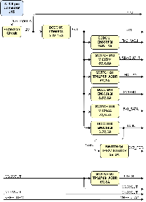
| Scroll Title |
|---|
| anchor | Figure_PWR_PD |
|---|
| title | Power Distribution |
|---|
|
| Scroll Ignore |
|---|
| draw.io Diagram |
|---|
| border | false |
|---|
| viewerToolbar | true |
|---|
| |
|---|
| fitWindow | false |
|---|
| diagramName | PD_TEF1002-01 |
|---|
| simpleViewer | false |
|---|
| links | auto |
|---|
| tbstyle | top |
|---|
| lbox | true |
|---|
| diagramWidth | 532 |
|---|
| revision | 46 |
|---|
|
|
| Scroll Only |
|---|
|
|
Power-On Sequence
...
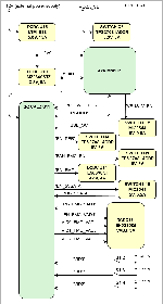
| Scroll Title |
|---|
| anchor | Figure_PWR_PS |
|---|
| title | Power Sequency |
|---|
|
| Scroll Ignore |
|---|
| draw.io Diagram |
|---|
| border | false |
|---|
| viewerToolbar | true |
|---|
| |
|---|
| fitWindow | false |
|---|
| diagramName | PS_TEF1002 |
|---|
| simpleViewer | false |
|---|
| links | auto |
|---|
| tbstyle | top |
|---|
| lbox | true |
|---|
| diagramWidth | 414448 |
|---|
| revision | 68 |
|---|
|
|
| Scroll Only |
|---|
|
|
Power Rails
In the following table power rails acceccible for in or output on any connectors are summarized.
| Scroll Title |
|---|
| anchor | Table_PWR_PR |
|---|
| title | Power Rails |
|---|
|
| Scroll Table Layout |
|---|
| orientation | portrait |
|---|
| sortDirection | ASC |
|---|
| repeatTableHeaders | default |
|---|
| sortByColumn | 1 |
|---|
| sortEnabled | false |
|---|
| cellHighlighting | true |
|---|
|
| Connector, Pins | Voltage | Direction | Notes |
|---|
| J15, 1,2,3 | 12V | IN | TEF1002 supply voltage | | J16, 1 | 5V | OUT | USB-VBUS_R | | J6, 1 | Depends on 4x5 Module | IN | Directly connected to B2B PSBATT pin | | J2, 2 | 5V | OUT | FMC Fan Connector | | JB1, 10,12 | 1,8V/3.3V | OUT | VCCIOA, selected by J4 | | JB1, 14,16 | 3.3V | OUT | Module supply voltage | | JB1, 40 | 1.8V | IN | Module 1.8V output | | JB1, 80 | Depends on 4x5 Module | OUT | Directly connected to pinheader J6 PSBATT | | JB1, 2,4,6 | 5V | OUT | Module power input | | JB2, 1,3,5,7 | 5V | OUT | Module power input | | JB2, 9,11 | 3.3V | IN | Module 3.3V output | | JB2, 2,4,6,8,10 | 0,8V ... 3.3V | OUT | Module VCCIOB, VCCIOC, VCCIOD connected to FMC VADJ | | JB2, 20 | Depends on 4x5 Module | IN | Module DDR power output | | JB2, 92 | Depends on 4x5 Module | IN | VREF_JTAG | | J13, 1,10 | 3.3V | OUT | FFA supply voltages | | J18, 1,10 | 3.3V | OUT | FFB supply voltages |
|
| Page properties |
|---|
|
- This section is optional and only for modules.
- use "include page" macro and link to the general B2B connector page of the module series, for example: 4 x 5 SoM LSHM B2B Connectors
| Include Page |
|---|
| PD:4 x 5 SoM LSHM B2B ConnectorsPD: |
|---|
| 4 x 5 SoM LSHM B2B Connectors |
|---|
|
|
...
| Scroll Title |
|---|
| anchor | Figure_RH_HRN |
|---|
| title | Hardware Revision Number |
|---|
|
| draw.io Diagram |
|---|
| border | true |
|---|
| viewerToolbar | true |
|---|
| |
|---|
| fitWindow | false |
|---|
| diagramName | HRN_TEF1002 |
|---|
| simpleViewer | false |
|---|
| diagramWidth | 406360 |
|---|
| revision | 12 |
|---|
|
|
Hardware revision number is printed on the PCB board next to the module model number separated by the dash.
...
| Scroll Title |
|---|
| anchor | Table_RH_DCH |
|---|
| title | Document change history. |
|---|
|
| Scroll Table Layout |
|---|
| orientation | portrait |
|---|
| sortDirection | ASC |
|---|
| repeatTableHeaders | default |
|---|
| sortByColumn | 1 |
|---|
| sortEnabled | false |
|---|
| cellHighlighting | true |
|---|
|
| Date | Revision | Contributor | Description |
|---|
| Page info |
|---|
| infoType | Modified date |
|---|
| dateFormat | yyyy-MM-dd |
|---|
| type | Flat |
|---|
|
| | Page info |
|---|
| infoType | Current version |
|---|
| prefix | v. |
|---|
| type | Flat |
|---|
| showVersions | false |
|---|
|
| | Page info |
|---|
| infoType | Modified by |
|---|
| type | Flat |
|---|
| showVersions | false |
|---|
|
| | | 2020-01-29 | v.28 | Martin Rohrmüller | | | 2019-09-06 | v.25 | Martin Rohrmüller | | -- | all | | Page info |
|---|
| infoType | Modified users |
|---|
| type | Flat |
|---|
| showVersions | false |
|---|
|
| |
|
...