Download PDF version of this document.
Table of Contents
Overview
The Trenz Electronic TEF1002-02 carrier is a baseboard for Trenz Electronic 4 x 5 SoMs. It is a PCIe x1 card and also hosts and LPC FMC connector.
See page "4 x 5 cm carriers" to get information about the SoMs supported by the TEF1002 carrier board.
Refer to trenz.org/tef1002-info for the current online version of this manual and other available documentation.
Key Features
Carrier for 4x5 modules
LPC FMC
- SFP+ connector
- PCIe x1
- SATA connector with pin 7 power configuration for SATADoM
- RJ45 Gigabit Ethernet connector
- micro-usb to JTAG/UART bridge
- 2x 8 lane high speed connectors (firefly)
- micro usb connector
- micro SD card connector
- 4x LED (2User, Power and Status)
- Module reset button
- 10x configuration/user dip switch
MAX10 CPLD
Block Diagram
TEF1002 block diagram
Main Components
TEF1002 main components
- ANSI/VITA 57.1 compliant FMC LPC connector, J1
- Cooling fan 5VDC M1 (45X5MM, 0.7W, 1.06CFM), M1
- SFP+ connector, J12
- PCIe x1 connector, J3
- SATA connector with pin 7 power configuration, J31
- Trenz Electronic 4 x 5 modules B2B connectors, JB1 ... JB3
- RJ45 Gigabit Ethernet connector, J9
- 2x high speed LVDS arrangement of connectors J11, J13, J14, J18
- Micro-USB2 connector, J10
- FTDI FT2232H USB2 to JTAG,UART/FIFO Bridge, U4
- Micro-USB2 connector, J16
- MAX10 10M08SAU169C8G CPLD, U11
- 6-pin 12V power connector, J15
- 5x2 CPLD JTAG pin header for TEI0004, J5
- 3x1 jumper pin header (select VCCIOA), J4
- 3x1 jumper pin header (select VCCA_SD), J7
- 3x1 pin header (VBAT), J6
- 2x3 pin header (MIO/PJTAG), J19
- Push button, S1
- 10x dip switch, S2, S3
- DCDC LTM4638 @5.0V, U9
- DCDC EN6338QI @3.3V, U10
- 2x green LED (user), D1, D2
- green LED (Power), D3
- green LED (Status), D4
- SD-Card connector (top loader),
- DCDC EN5335QI (FMC_VADJ), U1
- DCDC EN6338QI @3.3V (3V3FMC), U14
- SDIO Level shifter TXS02612, U3
Initial Delivery State
Storage device name | Content | Notes |
|---|---|---|
FTDI chip configuration EEPROM (93AA56B), U6 | Xilinx License | Do not overwrite, see warning in related section |
| MAX10 System Controller CPLD (10M08SAU169C8G), U14 | SC CPLD Firmware |
Initial delivery state of programmable devices on the module.
Control Signals
To get started with TEF1002 board, some basic control signals are essential and are described in the following table:
Control signal | Switch / Button / LED / Pin | Signal Schematic Names | Connected to | Functionality | Notes |
|---|---|---|---|---|---|
| FMC_VADJ voltage selection | DIP switches S2-1, S2-2, S2-3 | VID0 ... VID2 | SC CPLD U11, pins K6, J5, K5 | sets adjustable voltage for FMC connector | dependens on SC CPLD configuration |
| JTAG enable | DIP switch S2-4 | JTAGEN | SC CPLD U11, pin E5 | OFF: CPLD IOs | function in OFF position depends on SC CPLD configuration (JTAG on pin header J5 (for TEI0004) |
| Module JTAG select | DIP switch S2-5 | M_JTAGEN | B2B JB1, pin 90 | When S2-6 OFF: OFF: Module SOC JTAG enabled, ON: Module SC CPLD JTAG enabled | (JTAG via micro USB J10) |
| FMC JTAG select | DIP switch S2-6 | FMC_JTAG | SC CPLD U11,L3 | OFF: Module JTAG enabled (see S2-5) ON: FMC JTAG enabled | depends on SC CPLD configuration, (JTAG via micro USB J10) |
| Enable module power | DIP switch S2-7 | CM0 | SC CPLD U11, M3 | Module power. Set ON to enable module power. (Power management depends on module. ) | depends on SC CPLD configuration, only avialiable when 4x5 module installed |
| No sequenzing | DIP switch S2-8 | CM1 | SC CPLD U11, L2 | Module Power management. Set ON to disable module CPLD power management. Power management depends on module and not all modules support extended power management with CPLD. | depends on SC CPLD configuration, only avialiable when 4x5 module installed |
| Boot Mode | DIP switch S3-1 | CM2 | SC CPLD U11, K2 | Boot Mode for attached module (Default: OFF for primary SD boot and ON for primary QSPI boot. Depends also on module CPLD firmware). | depends on SC CPLD configuration, only avialiable when 4x5 module installed |
| FMC VADJ enable | DIP switch S3-2 | USR0 | SC CPLD U11, K1 | ON: FMC VADJ enable also without installed FMC Card OFF: FMC_FADJ only enabled when FMC installed. | dependens on SC CPLD configuration, only avialiable when 4x5 module installed |
| Reset | Push button S1 | BUTTON | SC CPLD U11, N6 | Module Reset, Low active module reset. Pin force Power one reset on FPGA/SoC. | depends on SC CPLD configuration |
| 2x User LED | Green LEDs D1, D2 | LED1, LED2 | SC CPLD U11, J5, K5 | Depends on User configuration, curenntly both off, if not otherwise programmed. | depends on SC CPLD configuration |
| Board power indicator | Green LED D3 | 3V3IN | B2B JB1, pin 14, 16 | ON: 3.3V on-board voltage available | - |
| Board status indicators | Green LED D4 | - | SC CPLD U11, pin C2 | ON: No failure. For other blinking status of this LED please refer to SC Firmware description. | dependens on SC CPLD configuration |
| Enable module power | SC CPLD U11, D11 | EN1 | B2B JB1, pin 27 | Module power. (Power management depends on module. ) | In standard Firmware connected to CM0 (see above) |
| No sequenzing | SC CPLD U11, E13 | NOSEQ | B2B JB1, pin 8 | Power management depends on module and not all modules support extended power management with CPLD. | In standard Firmware connected to CM1 (see above) |
| Boot Mode | SC CPLD U11, B11 | MODE | B2B JB1, pin 31 | Boot Mode for attached module. LOW for primary SD boot and HIGH for primary QSPI boot. (Depends also on module CPLD firmware). | In standard Firmware connected to CM2 (see above) |
| Module Reset | SC CPLD U11, E12 | RESIN | B2B JB2, pin 17 | Module Reset | In standard Firmware connected to BUTTON S1 (see above) |
TEF1002 Control Signals
Signals, Interfaces and Pins
Board to Board (B2B) I/Os
I/O signals connected to the B2B connector:
| B2B Connector | Interfaces | I/O Signal Count | Notes |
|---|---|---|---|
| JB1 | User IO | 15 single ended or 7 differential | TEF1002 CPLD |
| 16 single ended or 8 differential | FFA | ||
| 16 single ended or 8 differential | FFB | ||
| MIO/PJTAG/User IO | 4 | Pinheader J19 | |
| CPLD IO | 2 | Module CPLD IO to Carrier CPLD | |
| SD IO | 6 | - | |
| UART | 2 | - | |
| GbE PHY_MDIO + PHY_COM | 8 +1 | - | |
| Module Control | 5 | NOSEQ,, EN1, PGOOD, MODE, M_JTAGEN | |
JB3 | User IO | 12 single ended or 6 differential | LPC FMC |
| MGTs (RX+TX) | 4 | PCIe x1, SFP+, LPC FMC, SATA | |
MGTCLK | 1 differential | - | |
| CLK | 1 differential | - | |
| USB | 1 differnetial | OTG-D_P, OTG-D_N | |
| USB Control | 3 | OTG-ID | |
| JB2 | User IO | 56 single ended or 28 differential | LPC FMC |
| CLK | 2 differential | M2C | |
| JTAG | 4 | - |
General overview of B2B connectors
FMC LPC Connector
I/O signals and interfaces connected to the FPGA SoCs I/O bank and FMC connector J1:
| FMC Connector J2 Pins and Interfaces | I/O Signal Count | diff.-pairs count | Connected to | VCCIO voltage | Notes |
|---|---|---|---|---|---|
| I/O | 56 | 28 | B2B JB2 connector | FMC_VADJ | pins usable as single ended I/O's or differential pairs |
| 12 | 6 | B2B JB3 connector | FMC_VADJ | ||
| Multi Gigabit Transceiver | - | 2 | B2B JB3 connector, pin 19, 21 and 20, 22 | - | RX, TX |
| Gigabit Transceiver Clock | - | 1 | B2B JB3 connector, pin 31, 33 | - | |
| I²C (SDA, SCL) | 2 | - | SC CPLD U11, pin F9, J8 | 3V3IN | FMC I²C Geographical Address pins GA0 and GA1 set to GND. |
| JTAG | 5 | - | SC CPLD U11, pin N7, M8, F8, M7, N8 | 3V3IN | TDO, TMS, TCK, TDI, TRST |
| Clock Input | - | 2 | B2B JB3 connector | FMC_VADJ | 2x reference clock inputs |
| Control Signals | 2 | - | SC CPLD U11, pin M5, E9 | 3V3IN | 'PG_C2M', 'FMC_PRSNT' |
| Reference voltage (FMC_VREF) | - | - | - | - | Not Connected. |
FMC connector interface
SFP+ Interface
| Connector J12 Pins and Interfaces | I/O Signal Count | diff.-pairs count | Connected to | VCCIO voltage | Notes |
|---|---|---|---|---|---|
| Multi Gigabit Transceiver | - | 2 | B2B JB3 connector, pin 13, 15 and 14, 16 | - | RX, TX |
| Control | 6 | SC CPLD U11 | 3V3IN | TX_FAULT, TX_DIS, M-DEF0, RS0, RS1, LOS | |
| I²C (SDA, SCL) | 2 | - | SC CPLD U11, pin F9, J8 | 3V3IN | MUX via CPLD |
SFP+ interface
PCIe x1 card edge connector
| Connector J3 Pins and Interfaces | I/O Signal Count | diff.-pairs count | Connected to | VCCIO voltage | Notes |
|---|---|---|---|---|---|
| Multi Gigabit Transceiver | - | 2 | B2B JB3 connector, pin 25, 27 and 26, 28 | - | RX, TX |
| Clock | - | 1 | B2B JB3 connector, pin 32, 34 | - | |
| JTAG | 5 | - | SC CPLD U11, M12, M13, L11, N12, G10 | 3V3IN | TDO, TMS, TCK, TDI, TRST |
PCIe x1 card edge connector
SATA connector
The SATA connector includes the pin 7 power configuration. This means that pin 7 (usually GND) is connected to a power switch U15, applying 5V to this pin. This gives the possibility to use SATADoMs with pin 7 power configuration. If a standard SATA device is connected the short (Current >0.5A) of Pin7 to GND is detected by the powerswitch and the powerswitch is switched OFF by the CPLD until a powercycle of TEF1002. There is also the possibility to remove the pin 7 power configuration by removing R82 and assembling R83 (0 Ohm, 2012 (0805)).
| Connector J31 Pins and Interfaces | I/O Signal Count | diff.-pairs count | Connected to | VCCIO voltage | Notes |
|---|---|---|---|---|---|
| Multi Gigabit Transceiver, pin 5,6 and 2,3 | - | 2 | B2B JB3 connector, pin 7, 9 and 8, 10 | - | RX, TX |
| Pin 1,4 | - | - | GND | GND | - |
| Pin 7 | - | - | U15, pin 6,8 | 5V0_SATA | Connetion is via R82 0 Ohm resistor. |
SATA connector
High speed connectors FFA and FFB
There are two Firefly connector arrangements.
| Connector, Pins and Interfaces | I/O Signal Count | diff.-pairs count | Connected to | VCCIO voltage | Notes |
|---|---|---|---|---|---|
| FFA, J11 | - | 8 | B2B JB1 connector | - | - |
| FFA Control, J14 | 4 | - | SC CPLD U11, pin C10, C9, E8, B9 | 3V3IN | MPRS, MSEL, INTL, RSTL |
| FFA I2C, J14 | 2 | - | SC CPLD U11, pin E6, D6 | 3V3IN | |
| FFB, J11 | - | 8 | B2B JB1 connector | - | - |
| FFB Control, J14 | 4 | - | SC CPLD U11, pin A11, B10, A10, B9 | 3V3IN | MPRS, MSEL, INTL, RSTL |
| FFB I2C, J14 | 2 | - | SC CPLD U11, pin A9, D8 | 3V3IN |
FMC connector interface
The RSTL of both connectors are tied together.
microUSB JTAG/UART/FIFO Interface
The microUSB connector provides JTAG access to Module and FMC through the carriers USB to JTAG/UART/FIFO bridge. JTAG is routed for MUX to the CPLD. UART signals are connected to the module B2B connectors. For further description of the JTAG MUX see dip switches or SC CPLD Firmware. For other non-standard functionalitiers compare on-board connection and datasheet of FTDI FT2232H.
(CPLD JTAG access is via 2x5 pin header J5. See pin header description)
microUSB
| Connector J16, Pins and Interfaces | I/O Signal Count | LVDS-pairs count | Connected to | VCCIO voltage | Notes |
|---|---|---|---|---|---|
| DATA | - | 1 | B2B JB3 connector, pin 48, 50 | - | - |
| Power, Control | 3 | - | B2B JB3 pin 52, 54, 56 | - | OTG-ID, VBUS_V_EN, USB-VBUS |
MicroUSB J16
RJ45 - Ethernet MagJack
| Connector J9, Pins and Interfaces | I/O Signal Count | LVDS-pairs count | Connected to | VCCIO voltage | Notes |
|---|---|---|---|---|---|
| PHY_MDI | - | 4 | B2B JB1 connector, pin 3, 5, 9, 11, 15, 17, 21, 23 | - | - |
| LED1 | 2 | - | SC CPLD U11, pin B13, C12 | 3V3IN | green/yellow |
| LED2 | 2 | SC CPLD U11, pin D12, C13 | 3V3IN | green/yellow |
Gigabit Ethernet Connector
micro SD-Card connector
The micro SD-Card connector J8 is connected to a TXS02612 SDIO port expander, which is used as levelshifter. Depending on the modules IO Voltage of the IO Bank where the SD-Card is connected Jumper J7 has to be set.
| Connector J8 pin | Signal Schematic Name | Muxed to signal on Port Expander | Connected to | Notes |
|---|---|---|---|---|
| 2, DAT3 | SD-D3_LS | SD_D3 | B2B JB1, pin 18 | - |
3, CMD | SD-CMD_LS | SD_CMD | B2B JB1, pin 26 | - |
5, CLK | SD-CCLK_LS | SD_CCLK | B2B JB1, pin 28 | - |
7, DAT0 | SD-D0_LS | SD_D0 | B2B JB1, pin 24 | - |
8, DAT1 | SD-D1_LS | SD_D1 | B2B JB1, pin 22 | - |
1, DAT2 | SD-D2_LS | SD_D2 | B2B JB1, pin 20 | - |
| 9, CARD detect | SD-CD | - | U11, pin M1 | CPLD Firmware dependent, in default firmware not used |
micro SD-Card connector
On-board Peripherals
System Controller CPLD MAX10
The Intel/Altera MAX10 10M08SAU169C8G System Controller CPLD (U11) is the central system management unit where essential control signals are logically linked by the CPLD firmware. It generates output signals to control the system, the on-board peripherals and the interfaces. The JTAG and I2C between the on-board peripherals and the attached module are forwarded and controlled by the System Controller CPLD. A main tasks of the System Controller CPLD is the monitoring of the power-on sequence and configuring the state of the attached module. For detailed information, refer to the firmware documentation of the SC CPLD. Table below lists the SC CPLD I/O signals and pins:
| Signal name | SC CPLD Pin | Connected to | Function | Notes |
|---|---|---|---|---|
| ACBUS0 | A4 | FTDI U4, pin 22 | GPIO's available to user | (FIFO or other FTDI functions when FTDI reprogrammed) |
| ACBUS1 | B4 | FTDI U4, pin 23 | ||
| ACBUS2 | A5 | FTDI U4, pin 24 | ||
| ACBUS3 | B5 | FTDI U4, pin 25 | ||
| ACBUS4 | A6 | FTDI U4, pin 26 | ||
| ACBUS5 | B6 | FTDI U4, pin 27 | ||
| ACBUS6 | A7 | FTDI U4, pin 28 | ||
| ACBUS7 | A8 | FTDI U4, pin 29 | ||
| ADBUS4 | A2 | FTDI U4, pin 17 | ||
| ADBUS5 | B2 | FTDI U4, pin 18 | ||
| ADBUS6 | A3 | FTDI U4, pin 19 | ||
| ADBUS7 | B3 | FTDI U4, pin 20 | ||
| TCK | G2 | J5, 1 | CPLD JTAG signals from pin header | Other functions possible with non standard CPLD firmware. |
| TDI | F5 | J5, 9 | ||
| TDO | F6 | J5, 3 | ||
| TMS | G1 | J5, 5 | ||
| F_TCK | H3 | FTDI U4, pin 12 | Forwarded JTAG signals from FTDI chip. | (FIFO or other FTDI functions when FTDI reprogrammed) |
| F_TDI | H2 | FTDI U4, pin 13 | ||
| F_TDO | G4 | FTDI U4, pin 14 | ||
| F_TMS | F4 | FTDI U4, pin 15 | ||
| M_TCK | H5 | JB2, pin 100 | 4x5 Module JTAG | Bank with VCCIO is VREF_JTAG from Module |
| M_TDI | J2 | JB2, pin 96 | ||
| M_TDO | J1 | JB2, pin 98 | ||
| M_TMS | H6 | JB2, pin 94 | ||
| FMC_TCK | F8 | J1, pin D29 | FMC JTAG | TRST not used |
| FMC_TDI | M7 | J1, pin D30 | ||
| FMC_TDO | N7 | J1, pin D31 | ||
| FMC_TMS | M8 | J1, pin D33 | ||
| FMC_TRST | N8 | J1, pin D34 | ||
| PCIE_TCK | L11 | J3, pin A5 | PCIe JTAG | Currently not used |
| PCIE_TDI | N12 | J3, pin A6 | ||
| PCIE_TDO | M12 | J3, pin A7 | ||
| PCIE_TMS | M13 | J3, pin A8 | ||
| PCIE_TRST | G10 | J3, pin B9 | ||
| PCIE_PERST | F12 | J3, pin A11 | Indication that PCIe Bus is up (power, clocks) | |
| EN_FMC | L4 | U14, pin 9 | Enable switched 3.3V FMC power | pulled down |
| EN_FMC_VADJ | K7 | U1, pin 41 | Enable IO power FMC_VADJ | pulled down |
| EN_PER | F13 | Q4, pin 5 | Enable perepherie power 3V3_PER | pulled down |
| FAN_FMC_EN | K8 | Q1, pin 5 | Enable FMC FAN | floating during configuration (no pull down) |
| FMC_PG_C2M | M5 | J1, pin D1 | Indicate that all FMC related powers are up | pulled up |
| FMC_PRSNT_M2C_L | E9 | J1, pin H2 | Indicate if FMC installed | Low when FMC present |
| FMC_SCL | J8 | J1, pin C31 | I2C 2-wire serial bus | MUX in CPLD |
| FMC_SDA | F9 | J1, pin C30 | ||
| PG_FMC_VADJ | J6 | U1, pin 35 | Indicate FMC VADJ power is up | |
| FF_RSTL | B9 | J13, pin 6 and J18, pin 6 | Reset configuration | Both FF are resetted simultanously when pulled LOW |
| FFA_INTL | E8 | J13, pin 5 | Indicate interrrupt | LOW when fault condition, pulled up |
| FFA_MPRS | C10 | J13, pin 3 | Indicate FF Module installed | LOW when Module present, pulled up |
| FFA_MSEL | C9 | J13, pin 4 | Select attached FF Module | Pull low to use I2C |
| FFA_SCL | D6 | J13, pin 8 | I2C 2-wire serial bus | MUX in CPLD |
| FFA_SDA | E6 | J13, pin 7 | ||
| FFB_INTL | A10 | J18, pin 5 | Indicate interrrupt | LOW when fault condition, pulled up |
| FFB_MPRS | A11 | J18, pin 3 | Indicate FF Module installed | LOW when Module present, pulled up |
| FFB_MSEL | B10 | J18, pin 4 | Select attached FF Module | Pull low to use I2C |
| FFB_SCL | D8 | J18, pin 8 | I2C 2-wire serial bus | MUX in CPLD |
| FFB_SDA | A9 | J18, pin 7 | ||
| CPLD_IO_1 | B12 | JB1, pin 88 | (M)IOs from 4x5 Module | (M)IOs used for ETH PHY LEDs |
| CPLD_IO_2 | A12 | JB1, pin 92 | (M)IOs from 4x5 Module | |
| M10_RST | D1 | J5, pin 6 | Currently not used, functions possible with non standard CPLD firmware. | |
| M10_RX | E4 | J5, pin 8 | ||
| M10_TX | E3 | J5, pin 7 | ||
| EN1 | D11 | JB1, pin 27 | Enable on module power | Depends on module, on some similar to reset. |
| MODE | B11 | JB1, pin 31 | Boot Mode selection | For Zynq modules only. (LOW → SD, HIGH → primary QSPI) |
| NOSEQ | E13 | JB1, pin 8 | Disable module CPLD power management | Depends on module. On some modules no extended CPLD power management avaialble. |
| PGOOD | C11 | JB1, pin 29 | Power good signal | This is only for monitoring, do not use as powerenable! Pulled up. |
| RESIN | E12 | JB2, pin 17 | Module Reset | Aktive LOW |
| M3.3VOUT | M4 | JB2, pin 9 and 11 | Indicates module power is up | Used for perepherie power enable. Floating when no module installed (no pull down). |
| SFPA_LOS | M10 | J12, pin 8 | SFP signal loss | HIGH indicates signal loss |
| SFPA_M-DEF0 | F10 | J12, pin 6 | SFP modul absent | HIGH when module physically absent |
| SFPA_RS0 | N10 | J12, pin 7 | SFP rate select RX | LOW for 1000BASE-SX, HIGH for 10GBASE-SR |
| SFPA_RS1 | M11 | J12, pin 9 | SFP rate select TX | LOW for 1000BASE-SX, HIGH for 10GBASE-SR |
| SFPA_SCL | L10 | J12, pin 5 | I2C 2-wire serial bus | MUX in CPLD |
| SFPA_SDA | N9 | J12, pin 4 | ||
| SFPA_TX_DIS | M9 | J12, pin 3 | SFP transmitter disable | HIGH disables transmitter |
| SFPA_TX_FAULT | G9 | J12, pin 2 | Indicates SFP laser fault | HIGH indicates fault |
| VID0_FMC_VADJ | E10 | U1, pin 34 | FMC_VADJ Voltage select | Chip internal pulled up |
| VID1_FMC_VADJ | J7 | U1, pin 33 | ||
| VID2_FMC_VADJ | L5 | U1, pin 32 | ||
| VID0 | K6 | S2-1 | For FMC_VADJ Voltage select | |
| VID1 | N5 | S2-2 | ||
| VID2 | N4 | S2-3 | ||
| JTAGEN | E5 | S2-4 | ||
| FMC_JTAG | B1 | S2-6 | Enable FMC JTAG port | |
| CM0 | M3 | S2-7 | Dips for module control signals | |
| CM1 | L2 | S2-8 | ||
| CM2 | K2 | S3-1 | ||
| USR0 | C1 | S3-2 | User button | Currently used for override FMC VADJ enable |
| USB_OC | D9 | U12, pin 5 | USB overcurrent detection | |
| EN_5VSATA | E1 | U15, pin 1 | Enable SATA pin 7 power | |
| OC_VSATA | F1 | U15, pin 2 | Overcurrent detection SATA pin 7 power | |
| BUTTON | N6 | S1 | Reset button | |
| SD-CD | M1 | J8, pin 9 | SD-Card card detect switch | Currently not used |
| LED1 | J5 | D1 | User LED | |
| LED2 | K5 | D2 | ||
| - | C2 | D4 | Status LED | For further explanation see SC CPLD Firmware description |
| PHY_LED1 | D12 | J9 | Phy LEDs | |
| PHY_LED1R | C13 | J9 | ||
| PHY_LED2 | B13 | J9 | ||
| PHY_LED2R | C12 | J9 | ||
| A_00_N | J10 | JB1, pin 38 | Module to CPLD communication | Currently "three wire" I2C and RGPIO, see SC CPLD Firmware description |
| A_00_P | K10 | JB1, pin 36 | ||
| A_01_N | L12 | JB1, pin 35 | ||
| A_01_P | K11 | JB1, pin 37 | ||
| A_02_N | J12 | JB1, pin 41 | ||
| A_02_P | K12 | JB1, pin 39 | ||
| A_03_N | H10 | JB1, pin 44 | ||
| A_03_P | J9 | JB1, pin 42 | ||
| A_04_N | H13 | JB1, pin 47 | ||
| A_04_P | J13 | JB1, pin 45 | ||
| A_05_N | H8 | JB1, pin 57 | ||
| A_05_P | H9 | JB1, pin 55 | ||
| A_06_N | G12 | JB1, pin 49 | ||
| A_06_P | G13 | JB1, pin 51 | ||
| A_07 | L13 | JB1, pin 34 |
SC CPLD pin mapping
FTDI FT2232H
The TEF1002 board has an on-board microUSB 2.0 (J10) high-speed to JTAG/UART/FIFO IC FT2232H (U4) from FTDI. Channel A can be used as JTAG Interface (MPSSE) to program on module JTAG devices. Channel B can be used as UART Interface routed to the B2B connector. There is also a 256-byte serial EEPROM connected to the FT2232H chip pre-programmed with license code to support Xilinx programming tools.
Do not access the FT2232H EEPROM using FTDI programming tools. Doing so will erase normally invisible user EEPROM content and invalidate stored Xilinx JTAG license. Without this license the on-board JTAG will not be accessible any more with any Xilinx tools. Software tools from FTDI website do not warn or ask for confirmation before erasing user EEPROM content.
Refer to the FTDI datasheet to get information about other options of the FT2232H chip.
| FTDI U4 pin | Signal Schematic Name | Connected to, Pin | Function | Notes |
|---|---|---|---|---|
| Pin 22 | ACBUS0 | SC CPLD U4, A4 | GPIO's available to user | (FIFO or other FTDI functions when FTDI reprogrammed) |
| Pin 23 | ACBUS1 | SC CPLD U4, B4 | ||
| Pin 24 | ACBUS2 | SC CPLD U4, A5 | ||
| Pin 25 | ACBUS3 | SC CPLD U4, B5 | ||
| Pin 26 | ACBUS4 | SC CPLD U4, A6 | ||
| Pin 27 | ACBUS5 | SC CPLD U4, B6 | ||
| Pin 28 | ACBUS6 | SC CPLD U4, A7 | ||
| Pin 29 | ACBUS7 | SC CPLD U4, A8 | ||
| Pin 17 | ADBUS4 | SC CPLD U4, A2 | ||
| Pin 18 | ADBUS5 | SC CPLD U4, B2 | ||
| Pin 19 | ADBUS6 | SC CPLD U4, A3 | ||
| Pin 20 | ADBUS7 | SC CPLD U4, B3 | ||
| Pin 12 | F_TCK | SC CPLD U4, H3 | JTAG signals forward to SC CPLD U4 | (FIFO or other FTDI functions when FTDI reprogrammed) |
| Pin 13 | F_TDI | SC CPLD U4, H2 | ||
| Pin 14 | F_TDO | SC CPLD U4, G4 | ||
| Pin 15 | F_TMS | SC CPLD U4, F4 | ||
| Pin 32 | BDBUS0 | JB1, 91 | UART | |
| Pin 33 | BDBUS1 | JB1, 86 |
FT2232H interface connections
SDIO Port Expander
The TEF1002 is equipped with the Texas Instruments TXS02612 SDIO Port Expander (U3), which is used as a SDIO level shifter. Port A is connected to the B2B connector J1. The IO Voltage VCCA_SD of this port is selected by jumper J7 and has to be set according to the module attached. Port B0 is directly connected to the microSD Card connector (J8).
| Port Expander U3 pin | Signal Schematic Name | Connected to B2B Pin | Notes |
|---|---|---|---|
| Pin 6 | SD-D0 | JB1, Pin 24 | Signals levelshiftet to 3.3V and connected to card holder (J8) |
| Pin 7 | SD-D1 | JB1, Pin 22 | |
| Pin 1 | SD-D2 | JB1, Pin 20 | |
| Pin 3 | SD-D3 | JB1, Pin 18 | |
| Pin 4 | SD-CMD | JB1, Pin 26 | |
| Pin 9 | SD-CCLK | JB1, Pin 28 |
SDIO Port Expander connections
Configuration DIP-switches
S2 and S3 provide 10 dip-switchs for configuration purpurses. Some of them are hard wired others are SC CPLD firmware dependent. If Firmware dependet, the functions in Notes are for the actual delivery firmware. For further descriptions see firmware description.
| Switch | Signal Schematic Name | Connected to, Pin | Notes |
|---|---|---|---|
| S2-1 | VID0 | SC CPLD U11, K6 | SC CPLD firmware dependent, used for FMC_VADJ, see table below. Select according to the IO capabilites of attached 4x5 SoM and FMC. |
| S2-2 | VID1 | SC CPLD U11, N5 | |
| S2-3 | VID2 | SC CPLD U11, N4 | |
| S2-4 | JTAGEN | SC CPLD U11, E5 | ON TEF1002 SC CPLD JTAG; OFF CPLD IOs, hard wired. |
| S2-5 | M_JTAGEN | JB1, Pin 90 | When S2-6 OFF: OFF 4x5 module FPGA/SOC JTAG, ON 4x5 module CPLD JTAG, hard wired. |
| S2-6 | FMC_JTAG | SC CPLD U11, L3 | SC CPLD firmware dependent. ON: FMC JTAG; OFF 4x5 module JTAG, see S2-5. |
| S2-7 | CM0 | SC CPLD U11, M3 | SC CPLD firmware dependent, EN1 |
| S2-8 | CM1 | SC CPLD U11, L2 | SC CPLD firmware dependent, NOSEQ |
| S3-1 | CM2 | SC CPLD U11, K2 | SC CPLD firmware dependent, BOOT MODE |
| S3-2 | USR0 | SC CPLD U11, K1 | SC CPLD firmware dependent, Override FMC_EN_VADJ |
DIP-switches
| S2-1 | S2-2 | S2-3 | Output Voltage |
|---|---|---|---|
| OFF | OFF | OFF | 3.3V |
| OFF | OFF | ON | 2.5V |
| OFF | ON | OFF | 1.8V |
| OFF | ON | ON | 1.5V |
| ON | OFF | OFF | 1.25V |
| ON | OFF | ON | 1.2V |
| ON | ON | OFF | 0.8V |
FMC_VADJ selection
Jumper
There are two voltage select jumpers available. J4 is used to select the SDIO signal voltage and J7 is used to select VCCIOA IO Voltage. Both have to be selected according to the attached 4x5 module capabilities (See TRM of your module).
| Jumper | Power rail | 3.3V | 1.8V | Remark |
|---|---|---|---|---|
| J4 | VCCIOA | 1-2 | 2-3 | Powers 4x5 bank, where FFA and FFB high speed signals are connected. |
| J7 | VCCA_SD | 1-2 | 2-3 | Powers SDIO Levelshifter on 4x5 module side. |
Jumper positions
Push Button
There is on push button (S1) on the TEF1002. It is connected to the SC CPLD (U11 Pin N6). The function is firmware dependet. In the actual delivery firmware it is used as module reset connected to B2B JB2 Pin 17 (RESIN). For further descriptions see firmware description.
Pin Header
Pin header J5 (can be used with TEI0004 programming module or any other Quartus compatible JTAG programmer) for MAX10 CPLD Firmware programming. If dip switch S2-4 is set to OFF, JTAG pins can also be used as CPLD IOs, e.g. routed to FMC JTAG or as IO extension (not implemented in standard firmware).
| Pin | Signal Schematic Name | Connected to, pin | NOTE |
|---|---|---|---|
| 1 | TCK | U11, G2 | If dip switch S2-4 is set to OFF, this pins can be used as CPLD IOs (not implemented in standard firmware) |
| 2 | GND | - | - |
| 3 | TDO | U11, F6 | If dip switch S2-4 is set to OFF, this pins can be used as CPLD IOs (not implemented in standard firmware) |
| 4 | 3V3IN | - | - |
| 5 | TMS | U11, G1 | If dip switch S2-4 is set to OFF, this pins can be used as CPLD IOs (not implemented in standard firmware) |
| 6 | M10_RST | U11, D1 | (not implemented in standard firmware), usable as CPLD IO |
| 7 | M10_TX | U11, E3 | (not implemented in standard firmware), usable as CPLD IO |
| 8 | M10_RX | U11, E4 | (not implemented in standard firmware), usable as CPLD IO |
| 9 | TDI | U11, F5 | If dip switch S2-4 is set to OFF, this pins can be used as CPLD IOs (not implemented in standard firmware) |
| 10 | GND | - | - |
CPLD JTAG pin header J5
Pin 2 of the 3x1 pin header J6 is directly connected to the B2B connetor JB1 PSBATT pin. Pin to is connected to GND. This pin header can be used to supply the modules VBAT pin.
Check the TRM of the attached 4x5 Module for the correct Battery voltage. Do not short or swap polarity, this may damage the module!
Pinheader J19 is for PJTAG access or can be used as connector for the 4 IO pins.
| Pin | Signal Schematic Name | Connected to, pin | NOTE |
|---|---|---|---|
| 1 | PJTAG_TCK | JB1, 96 | Check 4x5 module TRM for capability of connected IO |
| 2 | PJTAG_TDO | JB1, 100 | Check 4x5 module TRM for capability of connected IO |
| 3 | PJTAG_TDI | JB1, 94 | Check 4x5 module TRM for capability of connected IO |
| 4 | PJTAG_TMS | JB1-98 | Check 4x5 module TRM for capability of connected IO |
| 5 | GND | - | - |
| 6 | M3.3VOUT | - | Module 3.3V |
PJTAG pin header J19
On-board LEDs
There are 4 green LEDs on the board, two of them are for user purpurses and controlabe via the RGPIO of the actual delivery firmware.
| LED | Connected to | Function | Notes |
|---|---|---|---|
| D1 | SC CPLD U11, Pin J5 | User LEDs | SC CPLD firmware dependet |
D2 | SC CPLD U11, Pin K5 | ||
| D3 | 3V3IN | Power | ON when 3.3V generated from 12V input is up |
| D4 | SC CPLD U11, Pin C2 | Status | SC CPLD firmware dependent, for further description see firmware description. |
LED Overview
Power and Power-On Sequence
Power Consumption
Power consumption depends on the attached 4x5 module and configuration, as well as FPGA design. Generally a power supply with minimum current capability of 3A at 12V for system startup is recommended.
Power Distribution Dependencies
Power Distribution
Power-On Sequence
Power up sequenz is depicted in the following figure. Most of the enables are handled by the SC CPLD and are therefore Firmware dependent. The Power up meets all criteria to power up 4x5 modules.
Power Sequency
Power Rails
In the following table power rails acceccible for in or output on any connectors are summarized.
| Connector, Pins | Voltage | Direction | Notes |
|---|---|---|---|
| J15, 1,2,3 | 12V | IN | TEF1002 supply voltage |
| J16, 1 | 5V | OUT | USB-VBUS_R |
| J6, 1 | Depends on 4x5 Module | IN | Directly connected to B2B PSBATT pin |
| J2, 2 | 5V | OUT | FMC Fan Connector |
| JB1, 10,12 | 1,8V/3.3V | OUT | VCCIOA, selected by J4 |
| JB1, 14,16 | 3.3V | OUT | Module supply voltage |
| JB1, 40 | 1.8V | IN | Module 1.8V output |
| JB1, 80 | Depends on 4x5 Module | OUT | Directly connected to pinheader J6 PSBATT |
| JB1, 2,4,6 | 5V | OUT | Module power input |
| JB2, 1,3,5,7 | 5V | OUT | Module power input |
| JB2, 9,11 | 3.3V | IN | Module 3.3V output |
| JB2, 2,4,6,8,10 | 0,8V ... 3.3V | OUT | Module VCCIOB, VCCIOC, VCCIOD connected to FMC VADJ |
| JB2, 20 | Depends on 4x5 Module | IN | Module DDR power output |
| JB2, 92 | Depends on 4x5 Module | IN | VREF_JTAG |
| J13, 1,10 | 3.3V | OUT | FFA supply voltages |
| J18, 1,10 | 3.3V | OUT | FFB supply voltages |
Power Rails
Technical Specifications
Absolute Maximum Ratings
| Parameter | Min | Max | Units | Reference Document |
|---|---|---|---|---|
VIN supply voltage | -0.3 | 20 | V | TPS6217 datasheet Note: voltage limitations are not valid for connected FMC module |
Storage temperature | -40 | +100 | °C | SML-P11 LED datasheet |
Module absolute maximum ratings.
Recommended Operating Conditions
| Parameter | Min | Max | Units | Reference Document |
|---|---|---|---|---|
| VIN supply voltage | 11.4 | 12.6 | V | 12V nominal, ANSI/VITA 57.1 power specification for FMC connector |
Board Operating Temperature Range | 0 | 85 | °C | 10M08SAU169C8G CPLD datasheet |
Recommended Operating Conditions.
Physical Dimensions
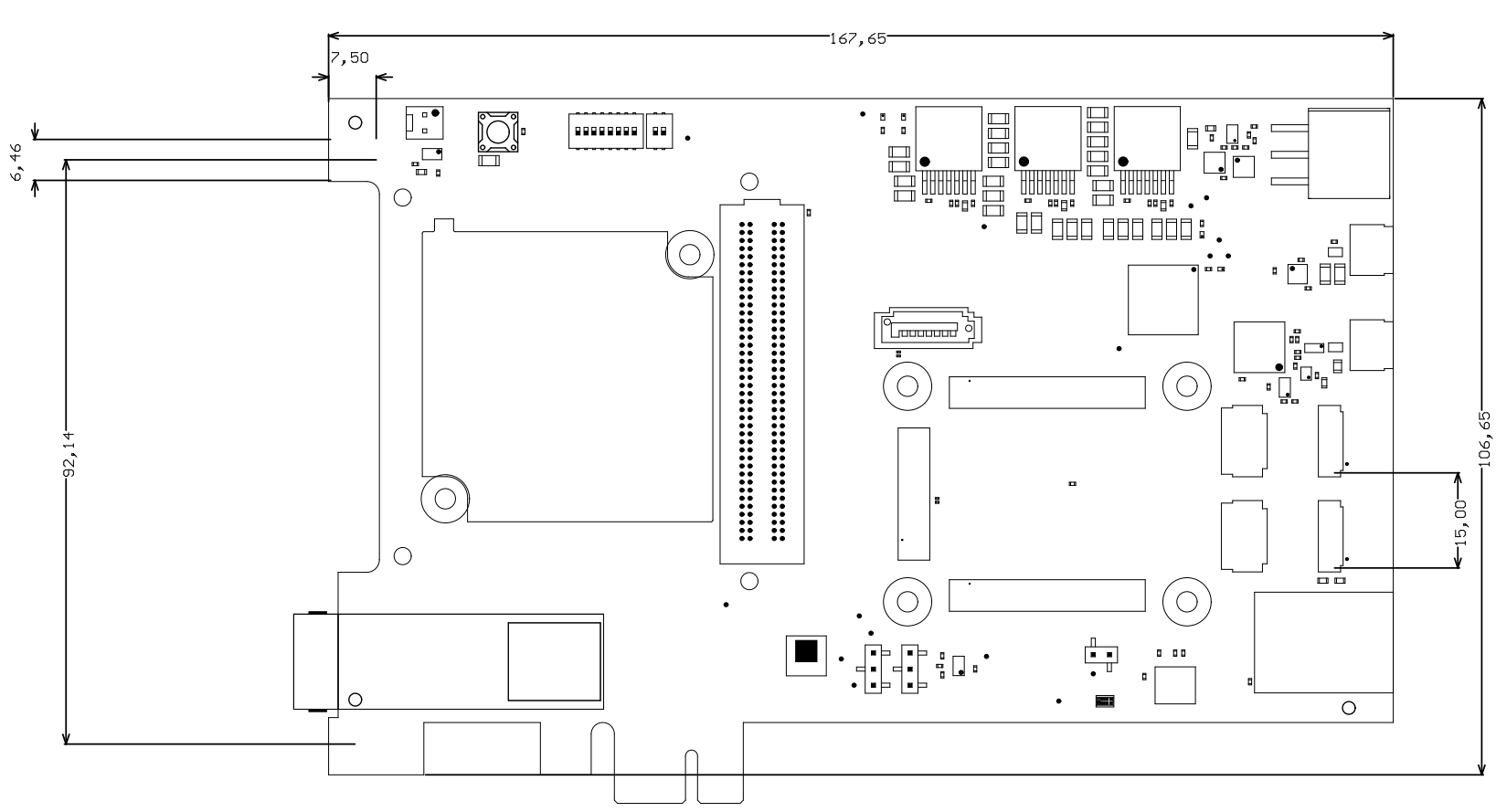
Physical dimensions drawing
Variants Currently In Production
| Trenz shop TEF1002 overview page | |
|---|---|
| English page | German page |
Trenz Electronic Shop Overview
Revision History
Hardware Revision History
| Date | Revision | Note | PCN | Documentation Link |
|---|---|---|---|---|
| 2020-01-29 | 02 | Prototypes | - | - |
| - | 01 | Prototypes | - | - |
Hardware Revision History
Hardware Revision Number
Hardware revision number is printed on the PCB board next to the module model number separated by the dash.
Document Change History
| Date | Revision | Contributor | Description |
|---|---|---|---|
| |||
| 2020-01-29 | v.28 | Martin Rohrmüller |
|
| 2019-09-06 | v.25 | Martin Rohrmüller |
|
-- | all |
|
Document change history.
Disclaimer
Data Privacy
Please also note our data protection declaration at https://www.trenz-electronic.de/en/Data-protection-Privacy
Document Warranty
The material contained in this document is provided “as is” and is subject to being changed at any time without notice. Trenz Electronic does not warrant the accuracy and completeness of the materials in this document. Further, to the maximum extent permitted by applicable law, Trenz Electronic disclaims all warranties, either express or implied, with regard to this document and any information contained herein, including but not limited to the implied warranties of merchantability, fitness for a particular purpose or non infringement of intellectual property. Trenz Electronic shall not be liable for errors or for incidental or consequential damages in connection with the furnishing, use, or performance of this document or of any information contained herein.
Limitation of Liability
In no event will Trenz Electronic, its suppliers, or other third parties mentioned in this document be liable for any damages whatsoever (including, without limitation, those resulting from lost profits, lost data or business interruption) arising out of the use, inability to use, or the results of use of this document, any documents linked to this document, or the materials or information contained at any or all such documents. If your use of the materials or information from this document results in the need for servicing, repair or correction of equipment or data, you assume all costs thereof.
Copyright Notice
No part of this manual may be reproduced in any form or by any means (including electronic storage and retrieval or translation into a foreign language) without prior agreement and written consent from Trenz Electronic.
Technology Licenses
The hardware / firmware / software described in this document are furnished under a license and may be used /modified / copied only in accordance with the terms of such license.
Environmental Protection
To confront directly with the responsibility toward the environment, the global community and eventually also oneself. Such a resolution should be integral part not only of everybody's life. Also enterprises shall be conscious of their social responsibility and contribute to the preservation of our common living space. That is why Trenz Electronic invests in the protection of our Environment.
REACH, RoHS and WEEE
REACH
Trenz Electronic is a manufacturer and a distributor of electronic products. It is therefore a so called downstream user in the sense of REACH. The products we supply to you are solely non-chemical products (goods). Moreover and under normal and reasonably foreseeable circumstances of application, the goods supplied to you shall not release any substance. For that, Trenz Electronic is obliged to neither register nor to provide safety data sheet. According to present knowledge and to best of our knowledge, no SVHC (Substances of Very High Concern) on the Candidate List are contained in our products. Furthermore, we will immediately and unsolicited inform our customers in compliance with REACH - Article 33 if any substance present in our goods (above a concentration of 0,1 % weight by weight) will be classified as SVHC by the European Chemicals Agency (ECHA).
RoHS
Trenz Electronic GmbH herewith declares that all its products are developed, manufactured and distributed RoHS compliant.
WEEE
Information for users within the European Union in accordance with Directive 2002/96/EC of the European Parliament and of the Council of 27 January 2003 on waste electrical and electronic equipment (WEEE).
Users of electrical and electronic equipment in private households are required not to dispose of waste electrical and electronic equipment as unsorted municipal waste and to collect such waste electrical and electronic equipment separately. By the 13 August 2005, Member States shall have ensured that systems are set up allowing final holders and distributors to return waste electrical and electronic equipment at least free of charge. Member States shall ensure the availability and accessibility of the necessary collection facilities. Separate collection is the precondition to ensure specific treatment and recycling of waste electrical and electronic equipment and is necessary to achieve the chosen level of protection of human health and the environment in the European Union. Consumers have to actively contribute to the success of such collection and the return of waste electrical and electronic equipment. Presence of hazardous substances in electrical and electronic equipment results in potential effects on the environment and human health. The symbol consisting of the crossed-out wheeled bin indicates separate collection for waste electrical and electronic equipment.
Trenz Electronic is registered under WEEE-Reg.-Nr. DE97922676.
Overview
Content Tools