...
| Scroll Title |
|---|
| anchor | Figure_OV_BD |
|---|
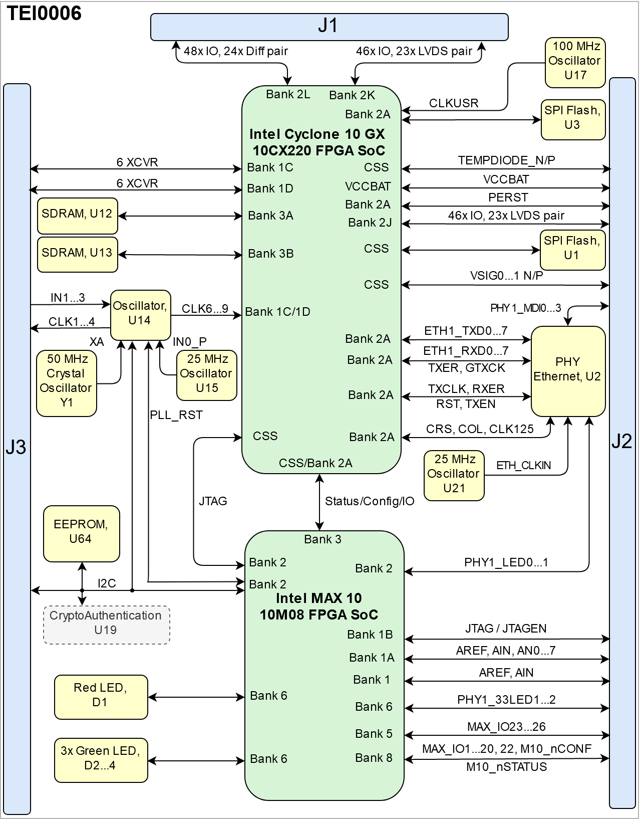
| title | TEI0006 block diagram |
|---|
|
| Scroll Ignore |
|---|
| draw.io Diagram |
|---|
| border | false |
|---|
| viewerToolbar | true |
|---|
| |
|---|
| fitWindow | false |
|---|
| diagramName | TEI0006_OV_BD |
|---|
| simpleViewer | false |
|---|
| links | auto |
|---|
| tbstyle | hidden |
|---|
| lbox | true |
|---|
| diagramWidth | 638 |
|---|
| revision | 1314 |
|---|
|
|
| Scroll Only |
|---|
|
|
Main Components
...
| Scroll Title |
|---|
| anchor | Table_SIP_B2B |
|---|
| title | General PL I/O to B2B connectors information |
|---|
|
| Scroll Table Layout |
|---|
| orientation | portrait |
|---|
| sortDirection | ASC |
|---|
| repeatTableHeaders | default |
|---|
| sortByColumn | 1 |
|---|
| sortEnabled | false |
|---|
| cellHighlighting | true |
|---|
|
| FPGA | FPGA Bank | B2B Connector | I/O Signal Count | Voltage Level | Notes |
|---|
| Intel Cyclone 10 GX | Bank 1C | J3 | 24 Single ended (12 Diff pair) | 0.95V |
| Bank 1D | J3 | 24 Single ended (12 Diff pair) | 0.95V |
| | Bank 2A | J2 | 1 Single ended | 1.8V | PERST | | Bank 2J | J2 | 46 Single ended (23 Diff pair) | 1.8V |
| | Bank 2K | J1 | 46 Single ended (23 Diff pair) | VCCIO2K |
| | Bank 2L | J1 | 46 Single ended (23 Diff pair) | 3.0V |
| | Bank 3A | - | - | 1.35V | VDD_DDR | | Bank 3B | - | - | 1.35V | VDD_DDR | | Intel Max 10 | Bank 1A | J2 | 8 Single ended | 3.3V |
| | Bank 1B | J2 | 5 Single ended | 3.3V |
| | Bank 2 | J3 | 2 Single ended | 1.8VIO |
| | Bank 3 | - | - | 1.8VIO |
| | Bank 5 | J2 | 4 Single ended | 3.3V |
| | Bank 6 | J2 | 2 Single ended | 3.3V |
| | Bank 8 | J2 | 25 Single ended | 3.3V |
|
|
JTAG Interface
JTAG access to the TEI0006 SoM through B2B connector JM2.
...
| Scroll Title |
|---|
| anchor | Table_OBP_MIOs |
|---|
| title | MIOs pins |
|---|
|
| Scroll Table Layout |
|---|
| orientation | portrait |
|---|
| sortDirection | ASC |
|---|
| repeatTableHeaders | default |
|---|
| sortByColumn | 1 |
|---|
| sortEnabled | false |
|---|
| cellHighlighting | true |
|---|
|
| MIO Pin | Connected to | B2B | Notes |
|---|
| MAX_IO1...22 | U18( Intel MAX 10) - Bank 8 | J2 |
| | MAX_IO23...26 | U18( Intel MAX 10) - Bank 8 | J2 |
|
|
On-board Peripherals
| Page properties |
|---|
|
Notes : - add subsection for every component which is important for design, for example:
- Two 100 Mbit Ethernet Transciever PHY
- USB PHY
- Programmable Clock Generator
- Oscillators
- eMMCs
- RTC
- FTDI
- ...
- DIP-Switches
- Buttons
- LEDs
|
...
| Scroll Title |
|---|
| anchor | Table_OBP |
|---|
| title | On board peripherals |
|---|
|
| Scroll Table Layout |
|---|
| orientation | portrait |
|---|
| sortDirection | ASC |
|---|
| repeatTableHeaders | default |
|---|
| sortByColumn | 1 |
|---|
| sortEnabled | false |
|---|
| cellHighlighting | true |
|---|
|
| Chip/Interface | Designator | Notes |
|---|
SPI Flash Memory | U1- U3 |
| | EEPROM | U64 |
| | SDRAM DDR3 Memory | U12...13 |
EEPROM | U64 | SPI Flash Memory | U1- U3 |
| | Ethernet Tranciever | U2- U14 |
| | Intel® Max 10 | U18 |
| User LEDs | D1...4 | D1 (Red), D2...4 (Green) | | Oscillators | U14, U15, U17, U21 |
|
|
Quad SPI Flash Memory
| Page properties |
|---|
|
Notes : Minimum and Maximum density of quad SPI flash must be mentioned for other assembly options. |
...
| Scroll Title |
|---|
| anchor | Table_OBP_I2C_EEPROM |
|---|
| title | I2C address for EEPROM |
|---|
|
| Scroll Table Layout |
|---|
| orientation | portrait |
|---|
| sortDirection | ASC |
|---|
| repeatTableHeaders | default |
|---|
| sortByColumn | 1 |
|---|
| sortEnabled | false |
|---|
| cellHighlighting | true |
|---|
|
| Pins | I2C Address | Designator | Notes |
|---|
| I2C_SCL, I2C_SDA | 0x53 | U64 |
|
LEDs
DDR3 SDRAM
| Page properties |
|---|
|
Notes : Minimum and Maximum density of DDR3 SDRAM must be mentioned for other assembly options. (pay attention to supported address length for DDR3) |
The TEI0006 SoM has two 1 Gb volatile DDR3 SDRAM IC for storing user application code and data.
- Part number: IS43TR16512BL
- Supply voltage: 1.35V
- Speed: 800MHz
- Temperature: 0 ° C to 95 ° C
Ethernet
| Scroll Title |
|---|
| anchor | Table_OBP_ETH |
|---|
| title | Ethernet PHY to Zynq SoC connections |
|---|
|
| Scroll Table Layout |
|---|
| orientation | portrait |
|---|
| sortDirection |
|---|
|
|
| Scroll Title |
|---|
| anchor | Table_OBP_LED |
|---|
| title | On-board LEDs |
|---|
|
| Scroll Table Layout |
|---|
| orientation | portrait |
|---|
| sortDirection | ASC |
|---|
| repeatTableHeaders | default |
|---|
| sortByColumn | 1 |
|---|
| sortEnabled | false |
|---|
| cellHighlighting | true |
|---|
|
Designator| Color | Active LevelNote | D1 | Red | LED_FP_1 | Active high | D2 | Green | LED_FP_2 | Active high | D3 | Green | LED_FP_3 | Active high | D4 | Green | LED_FP_4 | Active high | |
DDR3 SDRAM
| Page properties |
|---|
|
Notes : Minimum and Maximum density of DDR3 SDRAM must be mentioned for other assembly options. (pay attention to supported address length for DDR3) |
The TEI0006 SoM has two 1 Gb volatile DDR3 SDRAM IC for storing user application code and data.
- Part number: IS43TR16512BL
- Supply voltage: 1.35V
- Speed: 800MHz
- Temperature: 0 ° C to 95 ° C
Ethernet
| Signal Description |
|---|
PHY1_MDI0_P PHY1_MDI0_N | - - | J2-93 J2-91 |
| PHY1_MDI1_P PHY1_MDI1_N | - - | J2-87 J2-85 |
| PHY1_MDI2_P PHY1_MDI2_N | - - | J2-81 J2-79 |
| PHY1_MDI3_P PHY1_MDI3_N | - - | J2-75 J2-73 |
| | ETH1_RST | Bank 2A | - | Connected to DVDDH Voltage | | ETH1_MDC | Bank 2A | - | Connected to DVDDH Voltage | | ETH1_MDIO | Bank 2A | - | Connected to DVDDH Voltage | | ETH1_TXD0...7 | Bank 2A | - | Transfer | | ETH1_RXD0...7 | Bank 2A | - | Recieve | | ETH1_GTXCK | Bank 2A | - |
| | ETH1_TXCLK | Bank 2A | - |
| | ETH1_TXEN | - | - |
| | ETH1_TXER | - | - |
| | ETH1_RXCK |
|
| Scroll Title |
|---|
| anchor | Table_OBP_ETH |
|---|
| title | Ethernet PHY to Zynq SoC connections |
|---|
|
| Scroll Table Layout |
|---|
| orientation | portrait |
|---|
| sortDirection | ASC |
|---|
| repeatTableHeaders | default |
|---|
| sortByColumn | 1 |
|---|
| sortEnabled | false |
|---|
| cellHighlighting | true |
|---|
|
| Signal Name | Connected to | B2B | Signal Description |
|---|
PHY1_MDI0_P PHY1_MDI0_N | - - | J2-93 J2-91 | PHY1_MDI1_P PHY1_MDI1_N | - - | J2-87 J2-85 | PHY1_MDI2_P PHY1_MDI2_N | - - | J2-81 J2-79 | PHY1_MDI3_P PHY1_MDI3_N | - - | J2-75 J2-73 | ETH1_RST | Bank 2A | - | Connected to DVDDH VoltageGNG | | ETH1_MDCRXDV | Bank 2A | - | Connected to GNG | | PHY1_INT | - | - | Connected to DVDDH Voltage | | ETH1PHY1_MDIOLED1 | Bank 2A- | J2-69 | Connected to DVDDH Voltage | | PHY1_LED2 | - | J2-67 | Connected to GNG | | ETH1_CRS | BAnk | ETH1_TXD0...7 | Bank 2A | - | Transfer | | ETH1_RXD0...7 | Bank 2A | - | Recieve | ETH1_GTXCK | Bank 2A | - | ETH1_TXCLK | Bank 2A | - | ETH1_TXEN | - | - | ETH1_TXER | - | - | | ETH1_RXCK | Bank 2A | - | Connected to GNG | | ETH1_RXDV | Bank 2A | - | Connected to GNG | | PHY1_INT | - | - | Connected to DVDDH Voltage | | PHY1_LED1 | - | J2-69 | Connected to DVDDH Voltage | | PHY1_LED2 | - | J2-67 | Connected to GNG | ETH1_CRS | BAnk 2A | - | ETH1_XTAL_IN | ETH_CLKIN | - | From U21 (25MHz MEMS Oschillator)
| | ETH1_XTAL_IN | ETH_CLKIN | - | From U21 (25MHz MEMS Oschillator) |
|
LEDs
| Scroll Title |
|---|
| anchor | Table_OBP_LED |
|---|
| title | On-board LEDs |
|---|
|
| Scroll Table Layout |
|---|
| orientation | portrait |
|---|
| sortDirection | ASC |
|---|
| repeatTableHeaders | default |
|---|
| sortByColumn | 1 |
|---|
| sortEnabled | false |
|---|
| cellHighlighting | true |
|---|
|
| Designator | Color | Connected to | Active Level | Note |
|---|
| D1 | Red | LED_FP_1 | Active high |
| | D2 | Green | LED_FP_2 | Active high |
| | D3 | Green | LED_FP_3 | Active high |
| | D4 | Green | LED_FP_4 | Active high |
|
|
Clock Sources
| Scroll Title |
|---|
| anchor | Table_OBP_CLK |
|---|
| title | Osillators |
|---|
|
| Scroll Table Layout |
|---|
| orientation | portrait |
|---|
| sortDirection | ASC |
|---|
| repeatTableHeaders | default |
|---|
| sortByColumn | 1 |
|---|
| sortEnabled | false |
|---|
| cellHighlighting | true |
|---|
|
| Designator | Description | Frequency | Note |
|---|
| U21 | MEMS Oscillator | 25MHz |
| | U15 | MEMS Oscillator | 25MHz |
| | U17 | MEMS Oscillator | 48MHz |
| | U14 | Programmable Oscillator | Variable |
|
|
...