...
- Intel® Cyclone 10 GX Industrial [10CX220YF780I5G]
- Package: FBGA-780-FBGA
- Speed Grade: 5 (Fastest)
- Temperature: -40°C ~ 100°C
- Package compatible device 10CX150 and 10CX105 as assembly variant on request possible
- 2x SDRAM DDR3L Memory IC 8Gb, 800MHz
- 2x SPI Flash, 1 Gb
- 2x Transceiver Full Ethernet 64-QFN
- Programmable Oscillator
- Intel® MAX 10 as System Controller (CPLD)
- 2Kb EEPROM Memory
4x User LED
- I/O interfaces:
Board to Board (B2B):
- Plug-on module with 3 x 160-pin Samtec Razor Beam (ST5) connectors
Power Supply:
Others:
Dimension: 80m x 60m
Others:
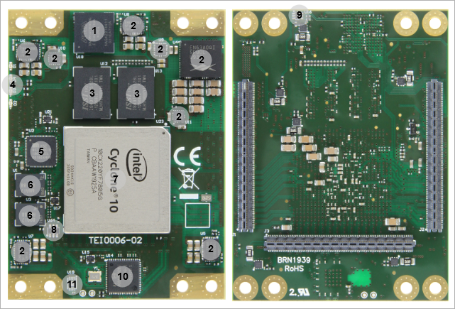
Block Diagram
| Page properties |
|---|
|
add drawIO object here.
|
...
| Scroll Title |
|---|
| anchor | Figure_OV_BD |
|---|
| title | TEI0006 main components |
|---|
|
| Scroll Ignore |
|---|
| draw.io Diagram |
|---|
| border | false |
|---|
| viewerToolbar | true |
|---|
| |
|---|
| fitWindow | false |
|---|
| diagramName | TEI0006_OV_MC |
|---|
| simpleViewer | false |
|---|
| links | auto |
|---|
| tbstyle | hidden |
|---|
| lbox | true |
|---|
| diagramWidth | 641 |
|---|
| revision | 3 |
|---|
|
|
|
- Intel® MAX 10, U18
- DC/DC convertor, U4...11
- SDRAM DDR3 Memory, U12...13
- User LEDs, D1...4
- Ethernet Tranciever, U2- U14
- SPI Flash Memory, U1- U3
- Intel® Cyclone 10 GX, U23
- EEPROM, U64
- Buffer, U16
Initial Delivery State
| Page properties |
|---|
|
Notes : Only components like EEPROM, QSPI flash and DDR3 can be initialized by default at manufacture. If there is no components which might have initial data ( possible on carrier) you must keep the table empty |
...
| Scroll Title |
|---|
| anchor | Table_OV_BP |
|---|
| title | Boot process. |
|---|
|
| Scroll Table Layout |
|---|
| orientation | portrait |
|---|
| sortDirection | ASC |
|---|
| repeatTableHeaders | default |
|---|
| sortByColumn | 1 |
|---|
| sortEnabled | false |
|---|
| cellHighlighting | true |
|---|
|
MODE Signal State | MSEL2 | MSEL1 | MSEL0 | Boot Mode |
|---|
MSEL[2:0] | 0 | 1 | 0 | AS x4 / Fast | | 0 | 1 | 1 | AS x1 / Standard | | 0 | 0 | 0 | PS and FPP/ Fast | | 0 | 0 | 1 | PS and FPP/ Standard |
|
By tying the CONF_DONE, nSTATUS, and nCONFIG pins together, the devices initialize and enter user mode at the same time. If any device in the chain detects an error, configuration stops for the entire chain and you must reconfigure all the devices. For example, if the first device in the chain flags an error on the nSTATUS pin, it resets the chain by pulling its nSTATUS pin low.
| Scroll Title |
|---|
| anchor | Table_OV_BP_CS |
|---|
| title | Configuration signals. |
|---|
|
| Scroll Table Layout |
|---|
| orientation | portrait |
|---|
| sortDirection | ASC |
|---|
| repeatTableHeaders | default |
|---|
| sortByColumn | 1 |
|---|
| sortEnabled | false |
|---|
| cellHighlighting | true |
|---|
|
| Signals | Connected to | Description | Note |
|---|
| nCONFIG | 1.8V | Configuration trigger | From U18( Intel MAX 10 Intel MAX 10) - Bank 3 | | CONF_DONE | 1.8V | Configuration done Configuration done | To U18( Intel MAX 10 Intel MAX 10) - Bank 3 | | nSTATUS | 1.8V | Configuration status status | To U18( Intel MAX 10 Intel MAX 10) - Bank 3 | | DCLK | U1,U3 | Configuration clock clock | To U1(Flash Memory) From U18( Intel MAX 10 Intel MAX 10) - Bank 3 | | AS_DATA0...3 | U1 | Configuration data | To From U1(Flash Memory) |
|
| Scroll Title |
|---|
| anchor | Table_OV_RST |
|---|
| title | Reset process. |
|---|
|
| Scroll Table Layout |
|---|
| orientation | portrait |
|---|
| sortDirection | ASC |
|---|
| repeatTableHeaders | default |
|---|
| sortByColumn | 1 |
|---|
| sortEnabled | false |
|---|
| cellHighlighting | true |
|---|
|
Signal | B2B | Connected to | Note |
|---|
PERST | J2-99 | Bank A2 |
|
|
...
| Scroll Title |
|---|
| anchor | Table_SIP_B2B |
|---|
| title | General PL I/O to B2B connectors information |
|---|
|
| Scroll Table Layout |
|---|
| orientation | portrait |
|---|
| sortDirection | ASC |
|---|
| repeatTableHeaders | default |
|---|
| sortByColumn | 1 |
|---|
| sortEnabled | false |
|---|
| cellHighlighting | true |
|---|
|
| FPGA | FPGA Bank | B2B Connector | I/O Signal Count | Voltage Level | Notes |
|---|
Intel Cyclone 10 GX | Bank 1C | J3 | 24 Single ended (12 Diff pair) | 0.95V | GXBL1C_RX0...5 N/P, GXBL1C_TX0...5 N/P | Bank 1D | J3 | 24 Single ended (12 Diff pair) | 0.95V | GXBL1D_RX0...5 N/P, GXBL1D_TX0...5 N/P | Bank 2A | J2 | 2 Single ended | 1.8V | PERST, CLKUSR | Bank 2J | J2 | 46 Single ended (23 Diff pair) | 1.8V |
| Bank 2K | J1 | 46 Single ended (23 Diff pair) | VCCIO2K |
| Bank 2L | J1 | 46 Single ended (23 Diff pair) | 3.0V |
| Bank 3A | - | - | 1.35V | VDD_DDR | Bank 3B | - | - | 1.35V | VDD_DDR | Intel Max 10 | Bank 1A | J2 | 8 Single ended | 3.3V |
| Bank 1B | J2 | 5 Single ended | 3.3V |
| Bank 2 | J3 | 2 Single ended | 1.8VIO |
| Bank 3 | - | - | 1.8VIO |
| Bank 5 | J2 | 4 Single ended | 3.3V |
| Bank 6 | J2 | 2 Single ended | 3.3V |
| Bank 8 | J2 | 25 Single ended | 3.3V |
|
|
JTAG Interface
JTAG access to the TEI0006 SoM through B2B connector JM2. JTAGEN is connected to 3.3V and after power on JTAG will be enabled.
| Scroll Title |
|---|
| anchor | Table_SIP_JTG |
|---|
| title | JTAG pins connection |
|---|
|
| Scroll Table Layout |
|---|
| orientation | portrait |
|---|
| sortDirection | ASC |
|---|
| repeatTableHeaders | default |
|---|
| sortByColumn | 1 |
|---|
| sortEnabled | false |
|---|
| cellHighlighting | true |
|---|
|
JTAG Signal | B2B Connector | Note |
|---|
| TMS | J2-160 |
| | TDI | J2-159 |
| | TDO | J2-158 |
| | TCK | J2-157 |
| | JTAGEN | J2-105 | Connected to 3.3V |
|
MIO Pins
| Page properties |
|---|
|
you must fill the table below with group of MIOs which are connected to a specific components or peripherals, you do not have to specify pins in B2B, Just mention which B2B is connected to MIOs. The rest is clear in the Schematic. Example: | MIO Pin | Connected to | B2B | Notes |
|---|
| MIO12...14 | SPI_CS , SPI_DQ0... SPI_DQ3 SPI_SCK | J2 | QSPI |
|
...
| Scroll Title |
|---|
| anchor | Table_OBP_MIOs |
|---|
| title | MIOs pins |
|---|
|
| Scroll Table Layout |
|---|
| orientation | portrait |
|---|
| sortDirection | ASC |
|---|
| repeatTableHeaders | default |
|---|
| sortByColumn | 1 |
|---|
| sortEnabled | false |
|---|
| cellHighlighting | true |
|---|
|
| MIO Pin | Connected to | B2B | Notes |
|---|
| MAX_IO1...22 | U18( Intel MAX 10) - Bank 8 | J2 |
| | MAX_IO23...26 | U18( Intel MAX 10) - Bank 8 | J2 |
|
|
On-board Peripherals
| Page properties |
|---|
|
Notes : - add subsection for every component which is important for design, for example:
- Two 100 Mbit Ethernet Transciever PHY
- USB PHY
- Programmable Clock Generator
- Oscillators
- eMMCs
- RTC
- FTDI
- ...
- DIP-Switches
- Buttons
- LEDs
|
...
| Scroll Title |
|---|
| anchor | Table_OBP |
|---|
| title | On board peripherals |
|---|
|
| Scroll Table Layout |
|---|
| orientation | portrait |
|---|
| sortDirection | ASC |
|---|
| repeatTableHeaders | default |
|---|
| sortByColumn | 1 |
|---|
| sortEnabled | false |
|---|
| cellHighlighting | true |
|---|
|
| Chip/Interface | Designator | Notes |
|---|
SPI DDR3 Tranciever |
...
QSPI Flash Memory
| Page properties |
|---|
|
Notes : Minimum and Maximum density of quad SPI flash must be mentioned for other assembly options. |
The TEI0006 is equipped with two Micron SPI flash memory. On-board SPI flash memory is used to store initial FPGA configuration. Besides FPGA configuration, remaining free flash memory can be used for user application and data storage. All four SPI data lines are connected to the FPGA allowing x1 or x4 data bus widths. Maximum data rate depends on the selected bus width and clock frequency.
| Scroll Title |
|---|
| anchor | Table_OBP_SPI |
|---|
| title | Quad SPI interface MIOs and pins |
|---|
|
| Scroll Table Layout |
|---|
| orientation | portrait |
|---|
| sortDirection | ASC |
|---|
| repeatTableHeaders | default |
|---|
| sortByColumn | 1 |
|---|
| sortEnabled | false |
|---|
| cellHighlighting | true |
|---|
|
| Designator | Schematic | Connected to | Notes |
|---|
U1
| NCSO | CSS Bank (Configuration Bank) | Used when you are not configuring using AS | | DCK | DCLK | AS Configuration Clock | | AS_DATA0 | CSS Bank (Configuration Bank) | AS Configuration Pin | | AS_DATA1 | CSS Bank (Configuration Bank) | AS Configuration Data | | AS_DATA2 | CSS Bank (Configuration Bank) | AS Configuration Data | | AS_DATA3 | CSS Bank (Configuration Bank) | AS Configuration Data | | U3 | QSPI_CS | Bank 2A |
| | QSPI_CK | Bank 2A |
| | QSPI_DATA0 | Bank 2A |
| | QSPI_DATA1 | Bank 2A |
| | QSPI_DATA2 | Bank 2A |
| | QSPI_DATA3 | Bank 2A |
|
|
...
| Scroll Title |
|---|
| anchor | Table_OBP_I2C_EEPROM |
|---|
| title | I2C address for EEPROM |
|---|
|
| Scroll Table Layout |
|---|
| orientation | portrait |
|---|
| sortDirection | ASC |
|---|
| repeatTableHeaders | default |
|---|
| sortByColumn | 1 |
|---|
| sortEnabled | false |
|---|
| cellHighlighting | true |
|---|
|
| Pins | I2C Address | Designator | Notes |
|---|
| I2C_SCL, I2C_SDA | 0x53 | U64 |
|
|
DDR3 SDRAM
| Page properties |
|---|
|
Notes : Minimum and Maximum density of DDR3 SDRAM must be mentioned for other assembly options. (pay attention to supported address length for DDR3) |
The TEI0006 SoM has two 1 Gb volatile DDR3 SDRAM IC for provided by Integrated Silicon Solution Inc for storing user application code and data.
- Part number: IS43TR16512BL
- Supply voltage: 1.35V
- Speed: 800MHz 800MHz
- Temperature: 0 0 ° C to 95 ° C
Ethernet PHY
| Scroll Title |
|---|
| anchor | Table_OBP_ETH |
|---|
| title | Ethernet PHY to Intel Cyclone 10 GX SoC connections |
|---|
|
| Scroll Table Layout |
|---|
| orientation | portrait |
|---|
| sortDirection | ASC |
|---|
| repeatTableHeaders | default |
|---|
| sortByColumn | 1 |
|---|
| sortEnabled | false |
|---|
| cellHighlighting | true |
|---|
|
| Signal Name | Connected to | B2B | Signal Description |
|---|
PHY1_MDI0_P PHY1_MDI0_N | - - | J2-93 J2-91 |
| PHY1_MDI1_P PHY1_MDI1_N | - - | J2-87 J2-85 |
| PHY1_MDI2_P PHY1_MDI2_N | - - | J2-81 J2-79 |
| PHY1_MDI3_P PHY1_MDI3_N | - - | J2-75 J2-73 |
| | ETH1_RST | Bank 2A | - | Connected to DVDDH Voltage | | ETH1_MDC | Bank 2A | - | Connected to DVDDH Voltage | | ETH1_MDIO | Bank 2A | - | Connected to DVDDH Voltage | | ETH1_TXD0...7 | Bank 2A | - | 8bit Transfer | | ETH1_RXD0...7 | Bank 2A | - | 8bit Recieve | | ETH1_GTXCK | Bank 2A | - |
| | ETH1_TXCLK | Bank 2A | - |
| | ETH1_TXEN | Bank 2A | - |
| | ETH1_TXER | Bank 2A | - |
| | ETH1_RXCK | Bank 2A | - | Connected to GNG | | ETH1_RXDV | Bank 2A | - | Connected to GNG | | PHY1_INT | - | - | Connected to DVDDH Voltage | | PHY1_LED1 | - | J2-69 | Connected to DVDDH Voltage | | PHY1_LED2 | - | J2-67 | Connected to GNG | | ETH1_CRS | Bank 2A | - |
| | ETH1_XTAL_IN | ETH_CLKIN | - | From U21 (25MHz MEMS Oschillator) |
|
...
| Scroll Title |
|---|
| anchor | Table_SIP_B2BMAX10 |
|---|
| title | General PL I/O to B2B connectors Intel MAX 10 banks information |
|---|
|
| Scroll Table Layout |
|---|
| orientation | portrait |
|---|
| sortDirection | ASC |
|---|
| repeatTableHeaders | default |
|---|
| sortByColumn | 1 |
|---|
| sortEnabled | false |
|---|
| cellHighlighting | true |
|---|
|
| Intel Max 10 Bank | Signals | Connected to | Description | Notes |
|---|
| Bank 1A | AIN0...7 | B2B- J2 |
|
| | Bank 1B | TCK, TDO, TMS, TDI, JTAGEN | B2B- J2 |
|
| | Bank 2 | PHY1_LED1 PHY1_LED2 | Ethernet PHY, U23 Ethernet PHY, U23 | Ethernet LED Ethernet LED | Tight to GND Tight to DVDDH | | F_TCK, F_TDO, F_TDI, F_TMS | Intel Cyclone 10 GX (U23) - Bank CSS | Intel Cyclone 10 JTAG signals |
| | I2C_SDA, I2C_SCL | EEPROM, U64 B2B, J3 Programmable Oscillator,U14 | I2C EEPROM signals |
| | PLL_RST | Programmable Oscillator, U14 | Oscillator reset signal |
| | Bank 3 | nSTATUS, nCONFIG, CONF_DONE | Intel Cyclone 10 GX (U23) - Bank CSS | Intel Cyclone 10 Configuration signals |
| | DCLK | Intel Cyclone 10 GX (U23) - Bank CSS SPI Flash, U1 | Intel Cyclone 10 Configuration clock from Flash memory |
| | MSEL0...1 | Intel Cyclone 10 GX (U23) - Bank CSS | Intel Cyclone 10 Configuration mode signals |
| | DEV_CLRN, INIT_DONE | Intel Cyclone 10 GX (U23)- Bank 2A |
|
| | M10_IO0...4 | Intel Cyclone 10 GX (U23) - Bank 2A |
|
| Bank 5
| DIS_GROUP1...4 | N- Channel MOSFET, T1...4 | Fast Discharching |
| | MAX_IO23...26 | B2B, J2 | Intel MAX 10 GPIO |
| PG_0.95V, EN_0.95V PG_1.8VIO, EN_1.8VIO | Voltage Regulator, U7 Voltage Regulator, U7 | Power control signals |
| Bank 6
| M10_CLK | 25MHz Oscillator, U2 | Intel MAX 10 Clock |
| VADJ_VS0...2, VADJ_EN PG_1.35V, EN_1.35V PG_1.8V, EN_1.8V PG_VTT, EN_VTT PG_0V9, EN_0V9 | Voltage Regulator, U11 Voltage Regulator, U8 Voltage Regulator, U5 Voltage Regulator, U9 Voltage Regulator, U4 | Power control signals |
| | PHY1_33LED1...2 | B2B, J2 | Ethernet LED |
| LED_FP_1 LED_FP_2...4 | D1 D2...4 | User LEDs | Red LED Green LED | | Bank 8 | M10_nSTATUS, M10_nCONFIG, M10_CONF_DONE | B2B, J2 | Intel MAX 10 configuration signals |
| | MAX_IO1...22 | B2B, J2 | Intel MAX 10 GPIO |
|
|
...
Power supply with minimum current capability of 2.5 1 A for system startup is recommended.
...
| Scroll Title |
|---|
| anchor | Table_PWR_PC |
|---|
| title | Power Consumption |
|---|
|
| Scroll Table Layout |
|---|
| orientation | portrait |
|---|
| sortDirection | ASC |
|---|
| repeatTableHeaders | default |
|---|
| sortByColumn | 1 |
|---|
| sortEnabled | false |
|---|
| cellHighlighting | true |
|---|
|
| Power Input PinFPGA | Typical Current |
|---|
| Intel Cyclone 10 GX | TBD* | | Intel MAX 10 | VIN | TBD* |
|
* TBD - To Be Determined
Power Distribution Dependencies
...
| Scroll Title |
|---|
| anchor | Table_TS_AMR |
|---|
| title | Absolute maximum ratings |
|---|
|
| Scroll Table Layout |
|---|
| orientation | portrait |
|---|
| sortDirection | ASC |
|---|
| repeatTableHeaders | default |
|---|
| sortByColumn | 1 |
|---|
| sortEnabled | false |
|---|
| cellHighlighting | true |
|---|
|
| Symbols | Description | Min | Max | Unit | Note |
|---|
| VCC | Core voltage power supply | -0.5 | 1.21 | V | Intel Cyclone 10 GX | | VCCP | Periphery circuitry and transceiver fabric interface power supply | -0.5 | 1.21 | V | Intel Cyclone 10 GX | | VCCERAM | Embedded memory power supply | -0.5 | 1.36 | V | Intel Cyclone 10 GX | | VCCPT | Power supply for programmable power technology and I/O pre-driver | -0.5 | 2.46 | V | Intel Cyclone 10 GX | | VCCIO | I/O buffers power supply | -0.5 | 4.10 | V | 3 V I/O Intel Cyclone 10 GX | | VCCA_PLL | Phase-locked loop (PLL) analog power supply | -0.5 | 2.46 | V | Intel Cyclone 10 GX | | VCCHVCCT_GXB | Transmitter Transceiver output buffer power supply | -0.5 | 12.3446 | V | VCCR_GXB | Intel Cyclone 10 GX | | VCC_ONE | Supply voltage for core and periphery through on-die voltage
regulator | -0.5 | 3.9 |
| Intel MAX 10 | | VCCA | Supply voltage for phase-locked loop (PLL) regulator and analog-todigital converter (ADC) block (analog)Receiver power supply | -0.5 | 13.349 |
| Intel MAX 10 | | VCCIO | Supply voltage for input and output buffers | V | VCCH_GXB | Transceiver output buffer power supply | -0.5 | 23.469 |
| VIntel MAX 10 | | T_STG | Storage temperature | -55 | 125 | °C |
|
|
...
| Scroll Title |
|---|
| anchor | Table_TS_ROC |
|---|
| title | Recommended operating conditions. |
|---|
|
| Scroll Table Layout |
|---|
| orientation | portrait |
|---|
| sortDirection | ASC |
|---|
| repeatTableHeaders | default |
|---|
| sortByColumn | 1 |
|---|
| sortEnabled | false |
|---|
| cellHighlighting | true |
|---|
|
| Parameter | Min | Max | Units | Reference Document |
|---|
| VCC | 0.87 | 0.93 | V | See Intel Cyclone 10 GX datasheet. | | VCCP | 0.87 | 0.93 | V | See Intel Cyclone 10 GX datasheet. | | VCCERAM | 0.87 | 0.93 | V | See Intel Cyclone 10 GX datasheet. | | VCCPT | 1.71 | 1.89 | V | See Intel Cyclone 10 GX datasheet. | | VCCPGM | 1.71 | 1.89 | V | See Intel Cyclone 10 GX datasheet. |
VCCP087093See Intel | See Intel Cyclone 10 GX datasheet. |
VCCERAM087093| 89 | V | See Intel Cyclone 10 GX datasheet. |
VCCPT| VCCH_GXB | 1.71 | 1.89 | V | See Intel |
Cyclone GX VCCPGM171189 Cyclone GX VCCIO28515 Cyclone GX VCCA_PLL | | VCCIO | 3.135 / 1.71 | 3.465 / 1.89 | V | See Intel |
Cyclone GX JSee Intel Cyclone GX
|
Physical Dimensions
Module size: 60 mm × 80 mm. Please download the assembly diagram for exact numbers.
Mating height with standard connectors: 5 mm.
- PCB thickness: 1.65 6 mm
| Page properties |
|---|
|
In 'Physical Dimension' section, top and button view of moduloe must be insterted, information regarding physical dimention can be obtained through webpage for product in Shop.Trenz, (Download> Documents> Assembly part)for every SoM. For Example: for Module TE0728, Physical Dimension information can be captured by snipping tools from the link below: https://www.trenz-electronic.de/fileadmin/docs/Trenz_Electronic/Modules_and_Module_Carriers/5.2x7.6/TE0745/REV02/Documents/AD-TE0745-02-30-1I.PDF
|
...
| Scroll Title |
|---|
| anchor | Table_RH_HRH |
|---|
| title | Hardware Revision History |
|---|
|
| Scroll Table Layout |
|---|
| orientation | portrait |
|---|
| sortDirection | ASC |
|---|
| repeatTableHeaders | default |
|---|
| sortByColumn | 1 |
|---|
| sortEnabled | false |
|---|
| cellHighlighting | true |
|---|
|
| Date | Revision | Changes | Documentation Link |
|---|
| 2018-0708-2710 | 01 | - | REV01 |
|
Hardware revision number can be found on the PCB board together with the module model number separated by the dash.
...