The Trenz Electronic TEI0006 is an Industrial industrial grade module based on Intel® Cyclone 10 GX. Intel Intel® Cyclone 10 GX device family delivers higher core, transceiver, and I/O performance than the previous generation of low cost FPGAs.
...
Intel® Cyclone 10 GX Industrial [10CX220YF780I5G]
Package: FBGA-780
Speed Grade: 5 (Fastest)
Temperature: -40°C ~ 100°C
Package compatible device 10CX150 and 10CX105 as assembly variant on request possible
2x SDRAM DDR3L Memory IC 8Gb8 Gbit (1 GByte), 800MHz
2x SPI Flash, 1 GbGbit (128 MByte)
1x 2x Transceiver Full Ethernet 64-QFN
Programmable Oscillator
Intel® MAX 10 as System Controller (CPLD)
2Kb 2Kbit EEPROM Memory
4x User LED
I/O interfaces:
284 GPIO
118 LVDS
12 XCVR
Board to Board (B2B):
Plug-on module with 3 x 160-pin Samtec Razor Beam (ST5) connectors
5 V Power Supply:
5V
Dimension: 80m x 60m
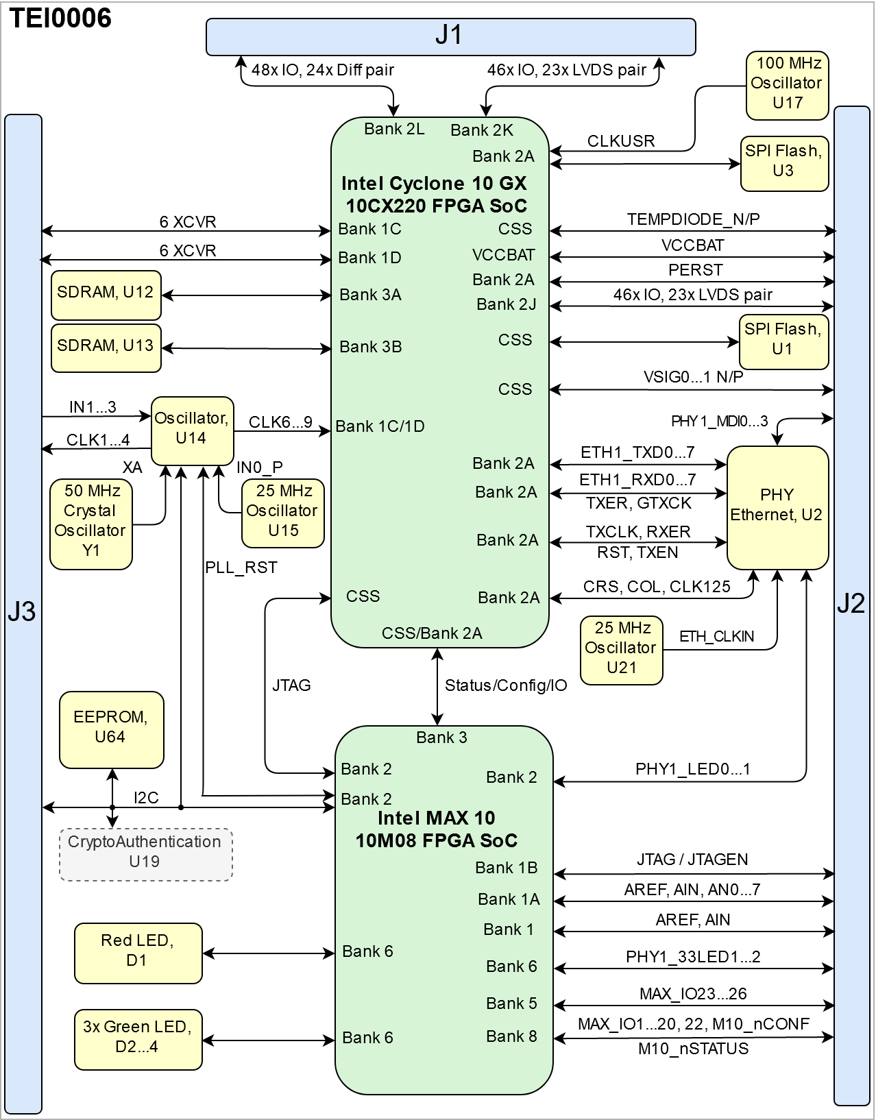
Block Diagram
...
Scroll Title
anchor
Figure_OV_BD
title
TEI0006 block diagram
Scroll Ignore
draw.io Diagram
border
false
viewerToolbar
true
fitWindow
false
diagramName
TEI0006_OV_BD
simpleViewer
false
links
auto
tbstyle
hidden
lbox
true
diagramWidth
638633
revision
1920
Scroll Only
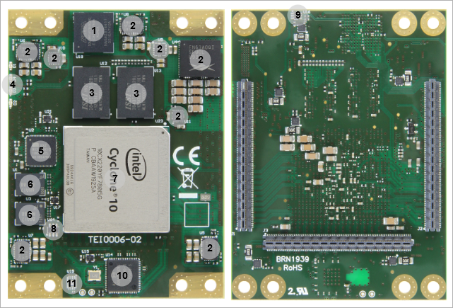
Main Components
...
Scroll Title
anchor
Figure_OV_BD
title
TEI0006 main components
Scroll Ignore
draw.io Diagram
border
false
viewerToolbar
true
fitWindow
false
diagramName
TEI0006_OV_MC
simpleViewer
false
links
auto
tbstyle
hidden
lbox
true
diagramWidth
641
revision
36
Scroll Only
Image Modified
Intel® MAX 10, U18
DC/DC convertor, U4...11
SDRAM DDR3 Memory, U12...13
User LEDs, D1...4
Ethernet TrancieverTransceiver, U2- U14
SPI Flash Memory, U1- U3
Intel® Cyclone 10 GX, U23
EEPROM, U64
Buffer, U16
Clock, U14
Initial Delivery State
Page properties
hidden
true
id
Comments
Notes :
Only components like EEPROM, QSPI flash and DDR3 can be initialized by default at manufacture.
If there is no components which might have initial data ( possible on carrier) you must keep the table empty
...
The TEI0006 module can be configured using different modes. Mode selection can be done using MSEL[2:0]. MSEL2 is potentially connected to GND so mode selection can be done using MSEL[1:0] which are connected to Bank 3 of Intel Max 10.
Scroll Title
anchor
Table_OV_BP
title
Boot process.
Scroll Table Layout
orientation
portrait
sortDirection
ASC
repeatTableHeaders
default
sortByColumn
1
sortEnabled
false
cellHighlighting
true
MODE Signal State
MSEL2
MSEL1
MSEL0
Boot Mode
MSEL[2:0]
0
1
0
AS x4 / Fast
0
1
1
AS x1 / Standard
0
0
0
PS and FPP / Fast
0
0
1
PS and FPP / Standard
...
Scroll Title
anchor
Table_OV_BP_CS
title
Configuration signals.
Scroll Table Layout
orientation
portrait
sortDirection
ASC
repeatTableHeaders
default
sortByColumn
1
sortEnabled
false
cellHighlighting
true
Signals
Connected to
Description
Note
nCONFIGNCONFIG
1.8V
Configuration trigger
From U18( Intel MAX 10) - Bank 3
CONF_DONE
1.8V
Configuration done
To U18( Intel MAX 10) - Bank 3
nSTATUSNSTATUS
1.8V
Configuration status
To U18( Intel MAX 10) - Bank 3
DCLK
U1,U3
Configuration clock
To U1(Flash Memory)
From U18( Intel MAX 10) - Bank 3
AS_DATA0...3
U1
Configuration data
From U1(Flash Memory)
...
Scroll Title
anchor
Table_SIP_B2B
title
General PL I/O to B2B connectors information
Scroll Table Layout
orientation
portrait
sortDirection
ASC
repeatTableHeaders
default
sortByColumn
1
sortEnabled
false
cellHighlighting
true
FPGA
FPGA Bank
B2B Connector
I/O Signal Count
Voltage Level
Notes
Intel Cyclone 10 GX
Bank 1C
J3
24 Single ended (12 Diff pair)
0.95V
GXBL1C_RX0...5 N/P, GXBL1C_TX0...5 N/P
Bank 1D
J3
24 Single ended (12 Diff pair)
0.95V
GXBL1D_RX0...5 N/P, GXBL1D_TX0...5 N/P
Bank 2A
J2
2 Single ended
1.8V
PERST, CLKUSR
Bank 2J
J2
46 Single ended (23 Diff pair)
1.8V
VCCIO2J
Bank 2K
J1
46 Single ended (23 Diff pair)
VCCIO2K
Bank 2L
J1
46 Single ended (23 Diff pair)
VADJ up to 3
.0V
V
Bank 3A
-
-
1.35V
VDD_DDR
Bank 3B
-
-
1.35V
VDD_DDR
Intel Max 10
Bank 1A
J2
8 Single ended
3.3V
Bank 1B
J2
5 Single ended
3.3V
Bank 2
J3
2 Single ended
1.8VIO
Bank 3
-
-
1.8VIO
Bank 5
J2
4 Single ended
3.3V
Bank 6
J2
2 Single ended
3.3V
Bank 8
J2
25
24 Single ended
3.3V
JTAG Interface
JTAG access to the TEI0006 SoM through B2B connector JM2J2. JTAGEN is connected pulled up to 3.3V and after power on, JTAG will be enabled.
Scroll Title
anchor
Table_SIP_JTG
title
JTAG pins connection
Scroll Table Layout
orientation
portrait
sortDirection
ASC
repeatTableHeaders
default
sortByColumn
1
sortEnabled
false
cellHighlighting
true
JTAG Signal
B2B Connector
Note
TMS
J2-160
TDI
J2-159
TDO
J2-158
TCK
J2-157
JTAGEN
J2-105
Connected Pulled up to 3.3V.
MIO Pins
Page properties
hidden
true
id
Comments
you must fill the table below with group of MIOs which are connected to a specific components or peripherals, you do not have to specify pins in B2B, Just mention which B2B is connected to MIOs. The rest is clear in the Schematic.
Example:
MIO Pin
Connected to
B2B
Notes
MIO12...14
SPI_CS , SPI_DQ0... SPI_DQ3
SPI_SCK
J2
QSPI
...
Scroll Title
anchor
Table_OBP_MIOs
title
MIOs pins
Scroll Table Layout
orientation
portrait
sortDirection
ASC
repeatTableHeaders
default
sortByColumn
1
sortEnabled
false
cellHighlighting
true
MIO Pin
Connected to
B2B
Notes
MAX_IO1...20, 22
U18( Intel MAX 10) - Bank 8
J2
MAX_IO23...26
U18( Intel MAX 10) - Bank 85
J2
On-board Peripherals
Page properties
hidden
true
id
Comments
Notes :
add subsection for every component which is important for design, for example:
Connected to Intel Max 10 (U18) - Bank 2, and Oscillator Si5345 (U14)
Scroll Title
anchor
Table_OBP_I2C_EEPROM
title
I2C address for EEPROM
Scroll Table Layout
orientation
portrait
sortDirection
ASC
repeatTableHeaders
default
sortByColumn
1
sortEnabled
false
cellHighlighting
true
Pins
I2C Address
Designator
Notes
I2C_SCL, I2C_SDA
0x53
U64
...
The TEI0006 SoM has two 1 Gb GByte volatile DDR3 SDRAM IC provided by Integrated Silicon Solution Inc for storing user application code and data.
Part number: IS43TR16512BL
Supply voltage: 1.35V
Speed: 800MHz
Temperature: 0 ° C -40 °C to 95 ° C°C
Ethernet PHY
Scroll Title
anchor
Table_OBP_ETH
title
Ethernet PHY to Intel Cyclone 10 GX SoC connections
Scroll Table Layout
orientation
portrait
sortDirection
ASC
repeatTableHeaders
default
sortByColumn
1
sortEnabled
false
cellHighlighting
true
Signal Name
Connected to
B2B
Signal Description
PHY1_MDI0_P
PHY1_MDI0_N
-
-
J2-93
J2-91
PHY1_MDI1_P
PHY1_MDI1_N
-
-
J2-87
J2-85
PHY1_MDI2_P
PHY1_MDI2_N
-
-
J2-81
J2-79
PHY1_MDI3_P
PHY1_MDI3_N
-
-
J2-75
J2-73
ETH1_RST
U23, Bank 2A
-
Connected Pulled-up to DVDDH Voltage.
ETH1_MDC
U23, Bank 2A
-
Connected Pulled-up to DVDDH Voltage.
ETH1_MDIO
U23, Bank 2A
-
Connected Pulled-up to DVDDH Voltage.
ETH1_TXD0...7
U23, Bank 2A
-
8bit 8 bit Transfer
ETH1_RXD0...7
U23, Bank 2A
-8bit Recieve
8 bit Receive
ETH1_GTXCK
U23, Bank 2A
-
ETH1_TXCLK
U23, Bank 2A
-
ETH1_TXEN
U23, Bank 2A
-
ETH1_TXER
U23, Bank 2A
-
ETH1_RXCK
U23, Bank 2A
-
Connected to GNGPulled-down to GND.
ETH1_RXDV
U23, Bank 2A
-
Connected to GNGPulled-down to GND.
PHY1_INT
-
-
Connected Pulled-up to DVDDH Voltage.
PHY1_LED1
U18, Bank 2
-J2
Pulled-69Connected up to DVDDH Voltage.
PHY1_LED2
U18, Bank 2
-J2
Pulled-67Connected to GNGdown to GND.
ETH1_CRS
U23, Bank 2A
-
ETH1_XTAL_IN
ETH_CLKIN
-
From U21 (25MHz MEMS Oschillator)
...
Scroll Title
anchor
Table_SIP_MAX10
title
Intel MAX 10 banks information
Scroll Table Layout
orientation
portrait
sortDirection
ASC
repeatTableHeaders
default
sortByColumn
1
sortEnabled
false
cellHighlighting
true
Intel Max 10 Bank
Signals
Connected to
Description
Notes
Bank 1A
AIN0...7
B2B- J2
Bank 1B
TCK, TDO, TMS, TDI, JTAGEN
B2B- J2
Bank 2
PHY1_LED1
PHY1_LED2
Ethernet PHY, U23U2
Ethernet PHY, U23U2
Ethernet LED
Ethernet LED
Pulled-up to DVDDH.
Pulled-down to GND.
Tight to GND
Tight to DVDDH
F_TCK, F_TDO, F_TDI, F_TMS
Intel Cyclone 10 GX (U23) - Bank CSS
Intel Cyclone 10 JTAG signals
I2C_SDA, I2C_SCL
EEPROM, U64
B2B, J3
Programmable Oscillator, U14
I2C EEPROM signals
PLL_RST
Programmable Oscillator, U14
Oscillator reset signal
Bank 3
nSTATUSNSTATUS, nCONFIGNCONFIG, CONF_DONE
Intel Cyclone 10 GX (U23) - Bank CSS
Intel Cyclone 10 Configuration signals
DCLK
Intel Cyclone 10 GX (U23) - Bank CSS
SPI Flash, U1
Intel Cyclone 10
Configuration clock from Flash memory
MSEL0...1
Intel Cyclone 10 GX (U23) - Bank CSS
Intel Cyclone 10
Configuration mode signals
DEV_CLRN, INIT_DONE
Intel Cyclone 10 GX (U23)- Bank 2A
M10_IO0...4
Intel Cyclone 10 GX (U23) - Bank 2A
Bank 5
DIS_GROUP1...4
N- Channel MOSFET, T1...4
Fast Discharching
MAX_IO23...26
B2B, J2
Intel MAX 10 GPIO
PG_0.95V, EN_0.95V
PG_1.8VIO, EN_1.8VIO
Voltage Regulator, U7
Voltage Regulator, U7U6
Power control signals
Bank 6
M10_CLK
25MHz Oscillator, U2U21
Intel MAX 10 Clock
VADJ_VS0...2, VADJ_EN
PG_1.35V, EN_1.35V
PG_1.8V, EN_1.8V
PG_VTT, EN_VTT
PG_0V9, EN_0V9
Voltage Regulator, U11
Voltage Regulator, U8
Voltage Regulator, U5
Voltage Regulator, U9
Voltage Regulator, U4
Power control signals
PHY1_33LED1...2
B2B, J2
Ethernet LED
LED_FP_1
LED_FP_2...4
D1
D2...4
User LEDs
Red LED
Green LED
Bank 8
M10_nSTATUS, M10_nCONFIG, M10_CONF_DONE
B2B, J2
Intel MAX 10 configuration signals
MAX_IO1...20, 22
B2B, J2
Intel MAX 10 GPIO
...
Scroll Title
anchor
Table_OBP_CLK_PO
title
Programmable Oscillator connections
Scroll Table Layout
orientation
portrait
sortDirection
ASC
repeatTableHeaders
default
sortByColumn
1
sortEnabled
false
cellHighlighting
true
Signals
Clock Type
In/ Out
Connected to
Frequency
Note
IN1IN0_P
IN1IN0_N
Differential
In
In
Oscillator, U15
GND
25 MHz
IN1..3
Differential
In
B2B, J3
Variable
XA
XB
Differential
Oscillator, U17
GND
48 MHz
CLK0
Differential
Out
Intel Cyclon 10 GX (U23)- Bank 2A
25MHz
CLK1...4
Differential
Out
B2B, J3
25MHz
REFCLK_EMIFP
Differential
Out
-Intel Cyclon 10 GX (U23)- Bank 3B
Variable
CLK6...7
Differential
Out
Intel Cyclon 10 GX (U23)- Bank 1D
Variable
CLK8...9
Differential
Out
Intel Cyclon 10 GX (U23)- Bank 1C
Variable
...
Scroll Title
anchor
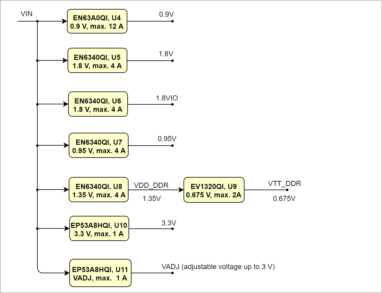
Figure_PWR_PD
title
Power Distribution
Scroll Ignore
draw.io Diagram
border
false
viewerToolbar
true
fitWindow
false
diagramDisplayName
lbox
true
revision
910
diagramName
TEI0006_PWR_PD
simpleViewer
false
width
links
auto
tbstyle
hidden
diagramWidth
639482
Scroll Only
Power-On Sequence
Voltage regulators can be enabled through U18 (Intel MAX 10) - Bank 5 and 6.
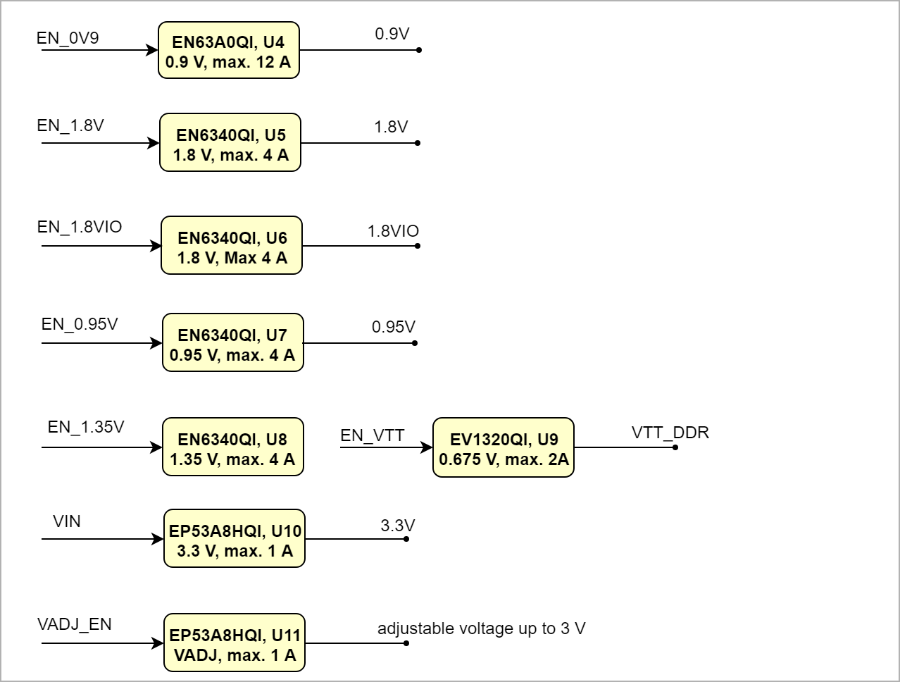
Scroll Title
anchor
Figure_PWR_PS
title
Power Sequence
Scroll Ignore
draw.io Diagram
border
false
viewerToolbar
true
fitWindow
false
diagramDisplayName
lbox
true
revision
58
diagramName
TEI0006_PWR_PS
simpleViewer
false
width
links
auto
tbstyle
hidden
diagramWidth
639482
Scroll Only
Power Rails
Scroll Title
anchor
Table_PWR_PR
title
Module power rails.
Scroll Table Layout
orientation
portrait
sortDirection
ASC
repeatTableHeaders
default
sortByColumn
1
sortEnabled
false
cellHighlighting
true
Power Rail Name
B2B Connector
JM1
J1 Pin
B2B Connector
JM2
J2 Pin
B2B Connector
JM3
J3 Pin
Voltage Level
Direction
Notes
VIN
145, 147,149, 151, 153, 155, 157, 159
-
-
5 V
Input
VCCIO2K
53, 54
-
-
1.2 V, 1.25 V, 1.35 V, 1.5 V, 1.8 V, 2.5 V or 3.0 V
Input
VADJ
140,142
-
-
3
adjustable between 1.
0
8 V - 3.0 V
Output
Voltages according to EP53A8HQI datasheet
VCCIO2J
-
29,30
-
1.2 V, 1.25 V, 1.35 V, 1.5 V, 1.8 V, 2.5 V or 3.0 V
Input
3.3V
-
149,150
-
3.3 V
Output
1.8_VIO
-
-
139
1.8 V
Output
Bank Voltages
Scroll Title
anchor
Table_PWR_BV
title
SoC bank voltages.
Scroll Table Layout
orientation
portrait
sortDirection
ASC
repeatTableHeaders
default
sortByColumn
1
sortEnabled
false
cellHighlighting
true
FPGA
FPGA Bank
Voltage Level
Notes
Intel Cyclone 10 GX
Bank 1C
0.95 V
Bank 1D
0.95 V
Bank 2A
1.8 V
1.8VIO
Bank 2J
1.2 V, 1.25 V, 1.8 V
VCCIO2J
Bank 2K
35 V, 1.5 V, 1.8 V
VCCIO2K
Bank 2L
, 2.5 V or 3.0 V
VCCIO2J
Bank
3A
2K
1.2 V, 1.25 V, 1.35 V, 1.5 V, 1.8 V, 2.5 V or 3.0 V
VCCIO2K
Bank 2L
adjustable between 1.8 V - 3.0 V
Voltages according to EP53A8HQI datasheet
Bank 3A
1.35 V
VDD_DDR
Bank 3B
1.35 V
VDD_DDR
Intel Max 10
Bank 1A
3.3 V
Bank 1B
3.3 V
Bank 2
1.8 V
1.8VIO
Bank 3
1.8 V
1.8VIO
Bank 5
3.3V
Bank 6
3.3V
Bank 8
3.3V
...
Operating Temperature: -55°C ~ 125°C Current Rating: 1.6 A per ContactNumber of Positions: ??Pin (2 pins powered)
Include Page
PD:4 x 6 SoM SS5/ST5 B2B Connectors
PD:4 x 6 SoM SS5/ST5 B2B Connectors
...
Scroll Title
anchor
Table_TS_AMR
title
Absolute maximum ratings
Scroll Table Layout
orientation
portrait
sortDirection
ASC
repeatTableHeaders
default
sortByColumn
1
sortEnabled
false
cellHighlighting
true
Symbols
Description
Min
Max
Unit
Note
VCC
VIN
Core voltage power
Power supply
-0.
5
3
1
6.
21
0
V
Intel Cyclone 10 GX
VCCP
Periphery circuitry and transceiver fabric interface power supply
-0.5
1.21
V
Intel Cyclone 10 GX
Detemined by U10.
VCCIO - 3 V I/O
I/O buffers
VCCERAM
Embedded memory
power supply
-0.5
1
4.
36
10
V
Intel Cyclone 10 GX
VCCIO - LVDS I/O
VCCPT
Power supply for programmable power technology and I/O pre-driverbuffers power supply
-0.5
2.46
V
Intel Cyclone 10 GX
VCCIO
I/O buffers power supply
VADJ
Adjustable voltage
-0.5
4.10
V
3
V
I/O
Intel Cyclone 10 GX
VCCAT_PLL
Phase-locked loop (PLL) analog power supply
-0.5
2.46
V
Intel Cyclone 10 GX
VCCH_GXB
Transceiver output buffer power supply
-0.5
2.46
V
Intel Cyclone 10 GX
VCC_ONE
Supply voltage for core and periphery through on voltageregulator
-0.5
3.9
V
Intel MAX 10
VCCA
Supply voltage for phase-locked loop (PLL) regulator and ADC
-0.5
3.9
V
Intel MAX 10
VCCIO
Supply voltage for input and output buffers
-0.5
3.9
V
Intel MAX 10
T_STG
Storage temperature
-55
125
°C
Recommended Operating Conditions
Operating temperature range depends also on customer design and cooling solution. Please contact us for options.
STG
Storage temperature
-40
85
°C
Recommended Operating Conditions
Operating temperature range depends also on customer design and cooling solution. Please contact us for options.
Scroll Title
anchor
Table_TS_ROC
title
Recommended operating conditions.
Scroll Table Layout
orientation
portrait
sortDirection
ASC
repeatTableHeaders
default
sortByColumn
1
sortEnabled
false
cellHighlighting
true
Parameter
Min
Max
Units
Reference Document
VIN
5.0
5.0
V
VCCIO
2.85
3.15
V
See Intel Cyclone 10 GX datasheet.
VADJ
2.85
3.15
V
VCCIO
Scroll Title
anchor
Table_TS_ROC
title
Recommended operating conditions.
Scroll Table Layout
orientation
portrait
sortDirection
ASC
repeatTableHeaders
default
sortByColumn
1
sortEnabled
false
cellHighlighting
true
Parameter
Min
Max
Units
Reference Document
VCC
0.87
0.93
V
See Intel Cyclone 10 GX datasheet.
VCCP
0.87
0.93
V
See Intel Cyclone 10 GX datasheet.
VCCERAM
0.87
0.93
V
See Intel Cyclone 10 GX datasheet.
VCCPT
1.71
1.89
V
See Intel Cyclone 10 GX datasheet.
VCCPGM
1.71
1.89
V
See Intel Cyclone 10 GX datasheet.
VCCIO
2.85
3.15
V
See Intel Cyclone 10 GX datasheet.
VCCA_PLL
1.71
1.89
V
See Intel Cyclone 10 GX datasheet.
VCCH_GXB
1.71
1.89
V
See Intel MAX 10 datasheet.
VCC_ONE
3.135
3.465
V
See Intel MAX 10 datasheet.
VCCA
3.135
3.465
V
See Intel MAX 10 datasheet.
VCCIO
3.135 / 1.71
3.465 / 1.89
V
See Intel MAX 10 datasheet.
T_OP
0
85
°C
See Intel MAX 10 datasheet.
Physical Dimensions
Module size: 60 mm × 80 mm. Please download the assembly diagram for exact numbers.
Mating height with standard connectors: 5 mm.
PCB thickness: 1.6 7 mm
Page properties
hidden
true
id
Comments
In 'Physical Dimension' section, top and button view of moduloe must be insterted, information regarding physical dimention can be obtained through webpage for product in Shop.Trenz, (Download> Documents> Assembly part)for every SoM.
For Example: for Module TE0728, Physical Dimension information can be captured by snipping tools from the link below: