...
| Scroll Title |
|---|
| anchor | Figure_OV_BD |
|---|
| title | TE... block diagram |
|---|
|
| Scroll Ignore |
|---|
| draw.io Diagram |
|---|
| border | truefalse |
|---|
| viewerToolbar | true |
|---|
| |
|---|
| fitWindow | false |
|---|
| diagramDisplayName | |
|---|
| lbox | true |
|---|
| revision | 3 |
|---|
| diagramName | BD_TEF1002-01 |
|---|
| simpleViewer | false |
|---|
| width | |
|---|
| links | auto |
|---|
| tbstyle | top |
|---|
| diagramWidth | 633 | revision | 1 |
|---|
|
|
| Scroll Only |
|---|
image link to the generate drawIO PNG file of this page. This is a workaround until scroll pdf export bug is fixed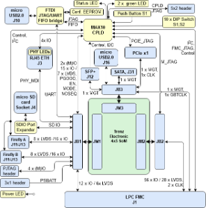 Image Added Image Added |
|
Main Components
...
| Scroll Title |
|---|
| anchor | Figure_OV_MC |
|---|
| title | TE... main components |
|---|
|
| Scroll Ignore |
|---|
add drawIO object here: Attention if you copy from other page, objects are only linked. |
| Scroll Only |
|---|
image link to the generate drawIO PNG file of this page. This is a workaround until scroll pdf export bug is fixed |
|
|---|
| draw.io Diagram |
|---|
| border | false |
|---|
| viewerToolbar | true |
|---|
| |
|---|
| fitWindow | false |
|---|
| diagramDisplayName | |
|---|
| lbox | true |
|---|
| revision | 4 |
|---|
| diagramName | TE1002-01_Main_components_top |
|---|
| simpleViewer | false |
|---|
| width | |
|---|
| links | auto |
|---|
| tbstyle | top |
|---|
| diagramWidth | 638 |
|---|
|
| draw.io Diagram |
|---|
| border | true |
|---|
| viewerToolbar | true |
|---|
| |
|---|
| fitWindow | false |
|---|
| diagramName | TE1002-01_Main_components_bottom |
|---|
| simpleViewer | false |
|---|
| width | |
|---|
| diagramWidth | 635 |
|---|
| revision | 4 |
|---|
|
|
| Scroll Only |
|---|
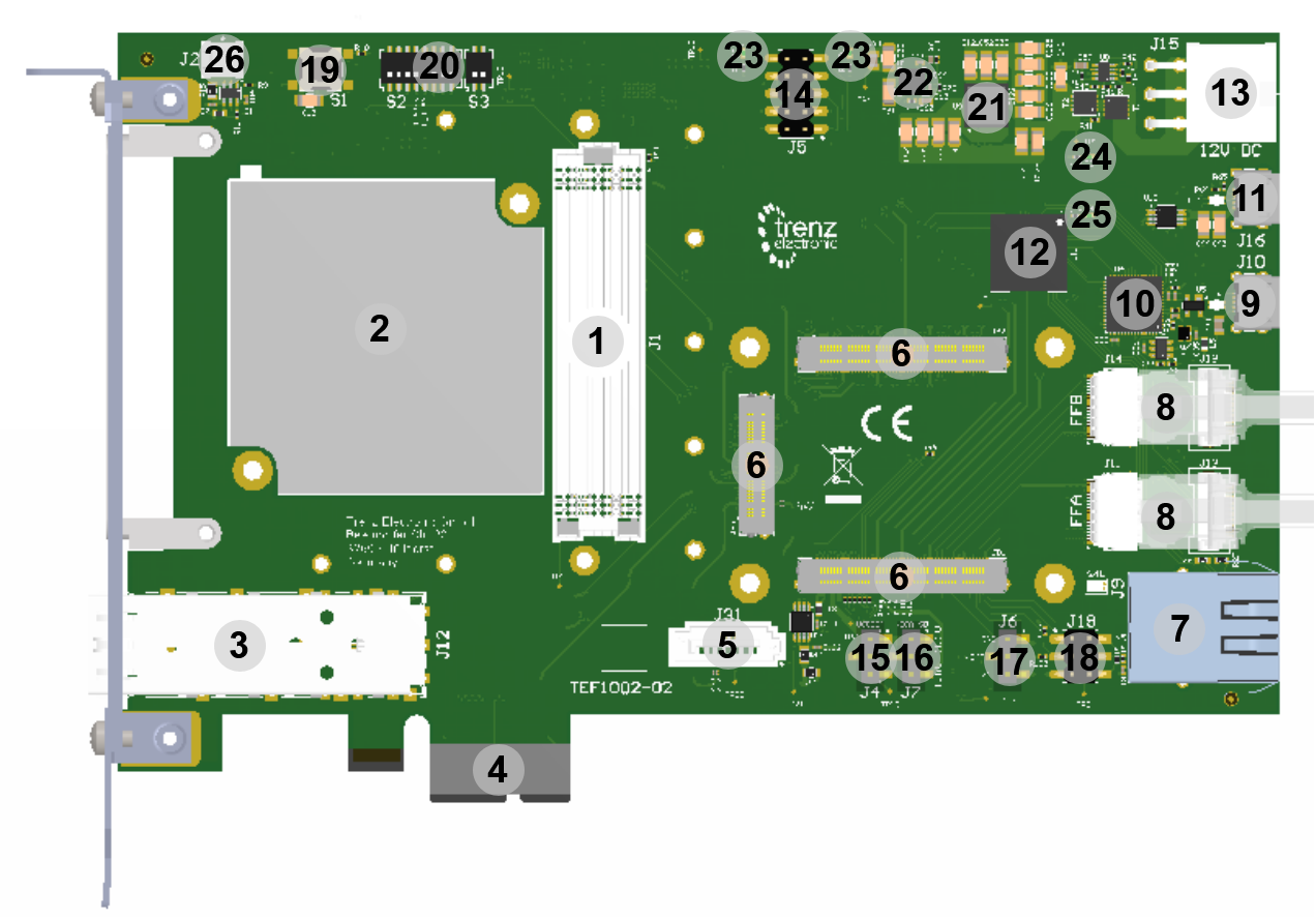 Image Added Image Added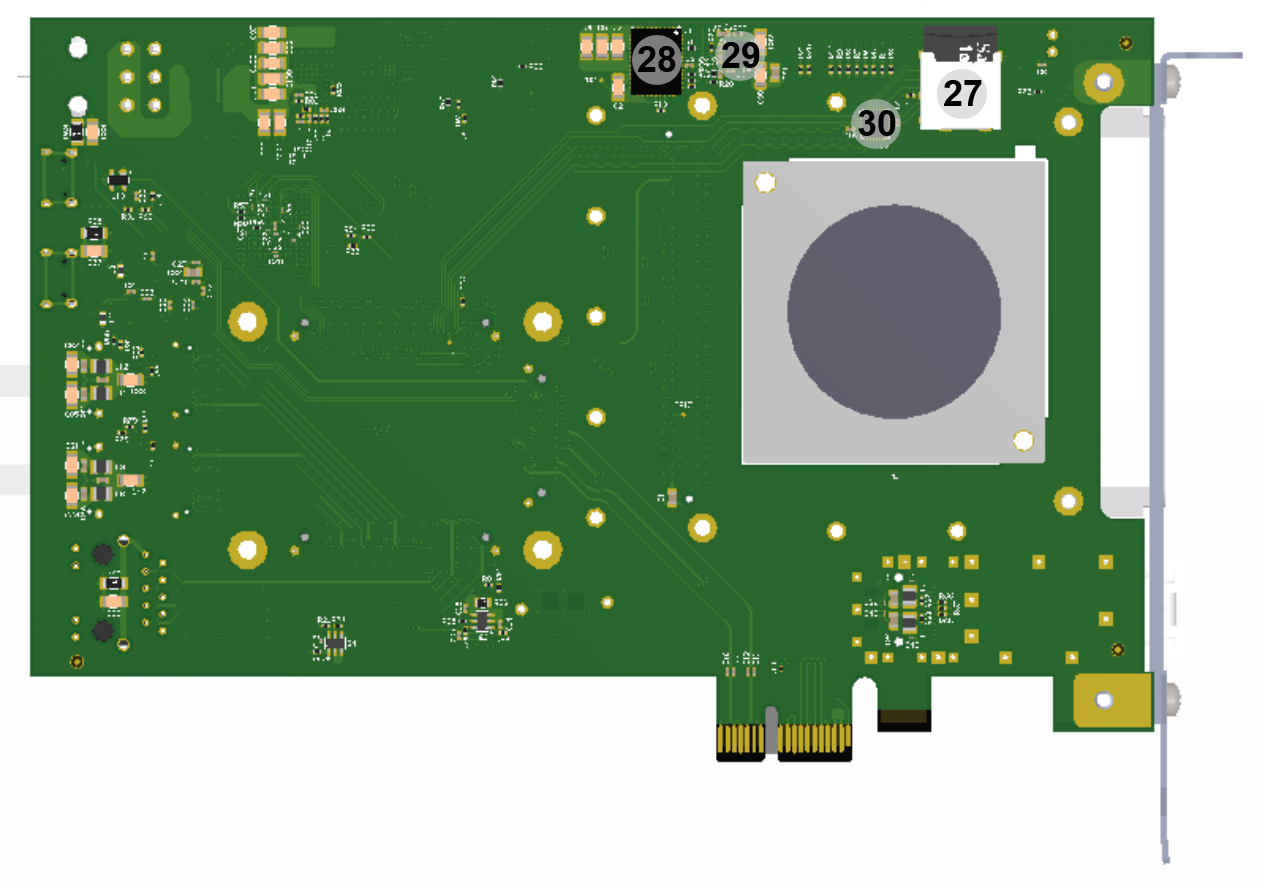 Image Added Image Added
|
|
- ANSI/VITA 57.1 compliant FMC LPC connector, J1
- Cooling fan 5VDC M1 (45X5MM, 0.7W, 1.06CFM), M1
- SFP+ connector, J12
- PCIe x1 connector, J3
- SATA connector, J31
- Trenz Electronic 4 x 5 modules B2B connectors, JB1 ... JB3
- RJ45 Gigabit Ethernet connector, J9
- 2x Firefly arrangement of connectors, J11, J13, J14, J18
- Micro-USB2 connector, J10
- FTDI FT2232H USB2 to JTAG,UART/FIFO Bridge, U4
- Micro-USB2 connector, J16
- MAX10 10M08SAU169C8G CPLD, U11
- 6-pin 12V power connector, J15
- 6x1 JTAG pin header (not fitted)
- 3x1 jumper pin header (select VCCIOA), J4
- 3x1 jumper pin header (select VCCA_SD), J7
- 2x1 pin header (VBAT), J6
- 2x5 1,27mm pitch pin header (PJTAG), J19
- Push button, S1
- 10x dip switch, S2, S3
- DCDC LMZ23605TZ @5.0V (5V0PER), U15
- DCDC LMZ23605TZ @5.0V (5V0), U9
- DCDC LMZ23605TZ @3.3V(3V3IN), U10
- 2x green LED (user), D1, D2
- green LED (Power), D3
- green LED (Status), D4
- SD-Card connector (top loader),
- DCDC EN5335QI (FMC_VADJ), U1
- DCDC EN6338QI @3.3V (3V3FMC), U14
- SDIO Level shifter TXS02612, U3
...
...
- ...
Initial Delivery State
| Scroll Title |
|---|
| anchor | Table_OV_IDS |
|---|
| title | Initial delivery state of programmable devices on the module. |
|---|
|
| Scroll Table Layout |
|---|
| orientation | portrait |
|---|
| sortDirection | ASC |
|---|
| repeatTableHeaders | default |
|---|
| style | |
|---|
| widths | |
|---|
| sortByColumn | 1 |
|---|
| sortEnabled | false |
|---|
| cellHighlighting | true |
|---|
|
Storage device name | Content | Notes |
|---|
.. | .. | .. | FTDI chip configuration EEPROM (93AA56B), U6 | Xilinx License | Do not overwrite, see warning in related section | | MAX10 System Controller CPLD (10M08SAU169C8G), U14 | SC CPLD Firmware | OTP Flash area | Empty | Not programmed. |
|
|
Control Signals
| Page properties |
|---|
|
- Overview of Boot Mode, Reset, Enables,
|
To get started with TEF1002 board, some basic control signals are essential and are described in the following table:
| Scroll Title |
|---|
| anchor | Table_OV_CS |
|---|
| title | TEF1002 Control Signals |
|---|
|
| Scroll Table Layout |
|---|
| orientation | portrait |
|---|
| sortDirection | ASC |
|---|
| repeatTableHeaders | default |
|---|
| style | |
|---|
| widths | |
|---|
| sortByColumn | 1 |
|---|
| sortEnabled | false |
|---|
| cellHighlighting | true |
|---|
|
Control signal | Switch / Button / LED / Pin | Signal Schematic Names | Connected to | Functionality | Notes |
|---|
| JTAG Enable | DIP switch S2-4 | JTAGEN | SC CPLD U11, pin E5 | OFF: SC CPLD JTAG enabled,
ON: Module/FMC JTAG enabled | - | | TODO!!!!! | DIP switch S2-4 |
|
|
|
| | BOOT MODE | SC CPLD U14, pin 27 | MODE | B2B JB1, pin 31 | Boot Mode for attached module (Flash or SD) | - | | Module Reset | SC CPLD U14, pin 13 | RESIN | B2B JB2, pin 17 | Module Reset | - | | Global Reset input | Push Button S2 | S2 | SC CPLD U14, pin 2 | Manual reset from user | - | | SD Card detection | SD Slot J8, pin 10 | SD_DETECT | SC CPLD U14, pin 40 | Detection Signal for inserted SD Card | Boot mode is set to SD Boot,
when SD Card is detected. | | Board status indicators | Red LEDs D1 ... D8 | ULED1 ... ULED8 | SC CPLD U14, pins
78, 77, 76, 16, 69, 68, 65, 64 | indicating various board and
module status / configuration | Refer to the firmware documentation of the SC CPLD
U14 and to the subsection 'LEDs' in section 'On-board Peripherals'
for more details and current functionality. | | Board 3.3V power indicator | Green LED D22 | 3V3IN | B2B JB1, pin 14, 16 | ON: 3.3V on-board voltage available | - | | FMC_VADJ voltage selection | DIP switches S4-1, S4-2, S4-3 | VID0 ... VID2 | SC CPLD U14, pins 34, 35, 38 | sets adjustable voltage for FMC connector | - | | I²C control / FMC_VADJ voltage selection | DIP switches S3-2, S3-1 | CM0, CM1 | SC CPLD U14, pins 99, 1 | enabling / disabling I²C control of board functionalities,
sets FMC_VADJ voltage (only 3 steps),
available to user if FMC_VADJ set by DIP-switch S4 | Refer to the firmware documentation of the SC CPLD
U14 and and to the subsection 'DIP switches' in section 'On-board
Peripherals' for current functionality and more details. |
|
Signals, Interfaces and Pins
...