...
| Scroll Title |
|---|
| anchor | Table_SIP_CPLD |
|---|
| title | SC CPLD pin mapping |
|---|
|
| Scroll Table Layout |
|---|
| orientation | portrait |
|---|
| sortDirection | ASC |
|---|
| repeatTableHeaders | default |
|---|
| style | |
|---|
| widths | |
|---|
| sortByColumn | 1 |
|---|
| sortEnabled | false |
|---|
| cellHighlighting | true |
|---|
|
| Signal name | SC CPLD Pin | Connected to | Function | Notes |
|---|
| ACBUS0 | A4 | FTDI U4, pin 22 | GPIO's available to user
| (FIFO or other FTDI functions when FTDI reprogrammed)
| | ACBUS1 | B4 | FTDI U4, pin 23 | | ACBUS2 | A5 | FTDI U4, pin 24 | | ACBUS3 | B5 | FTDI U4, pin 25 | | ACBUS4 | A6 | FTDI U4, pin 26 | | ACBUS5 | B6 | FTDI U4, pin 27 | | ACBUS6 | A7 | FTDI U4, pin 28 | | ACBUS7 | A8 | FTDI U4, pin 29 | | ADBUS4 | A2 | FTDI U4, pin 17 | | ADBUS5 | B2 | FTDI U4, pin 18 | | ADBUS6 | A3 | FTDI U4, pin 19 | | ADBUS7 | B3 | FTDI U4, pin 20 | | TCK | G2 | FTDI U4, pin 12 | Forwarded JTAG signals from FTDI chip.
| (FIFO or other FTDI functions when FTDI reprogrammed)
| | TDI | F5 | FTDI U4, pin 13 | | TDO | F6 | FTDI U4, pin 14 | | TMS | G1 | FTDI U4, pin 15 | | M_TCK | H5 | JB2, pin 100 | 4x5 Module JTAG
| Bank with VCCIO is VREF_JTAG from Module
| | M_TDI | J2 | JB2, pin 96 | | M_TDO | J1 | JB2, pin 98 | | M_TMS | H6 | JB2, pin 94 | | FMC_TCK | F8 | J1, pin D29 | FMC JTAG
| TRST not used
| | FMC_TDI | M7 | J1, pin D30 | | FMC_TDO | N7 | J1, pin D31 | | FMC_TMS | M8 | J1, pin D33 | | FMC_TRST | N8 | J1, pin D34 | | PCIE_TCK | L11 | J3, pin A5 | PCIe JTAG
| Currently not used
| | PCIE_TDI | N12 | J3, pin A6 | | PCIE_TDO | M12 | J3, pin A7 | | PCIE_TMS | M13 | J3, pin A8 | | PCIE_TRST | G10 | J3, pin B9 | | PCIE_PERST | F12 | J3, pin A11 | Indication that PCIe Bus is up (power, clocks) |
| | EN_FMC | L4 | U14, pin 9 | Enable switched 3.3V FMC power | pulled down | | EN_FMC_VADJ | K7 | U1, pin 41 | Enable IO power FMC_VADJ | pulled down | | EN_PER | F13 | Q4, pin 5 | Enable perepherie power 3V3_PER | pulled down | | FAN_FMC_EN | K8 | Q1, pin 5 | Enable FMC FAN |
| | FMC_PG_C2M | M5 | J1, pin D1 | Indicate that all FMC related powers are up | pulled up | | FMC_PRSNT_M2C_L | E9 | J1, pin H2 | Indicate if FMC installed | Low when FMC present | | FMC_SCL | J8 | J1, pin C31 | I2C 2-wire serial bus | MUX in CPLD | | FMC_SDA | F9 | J1, pin C30 | | PG_FMC_VADJ | J6 | U1, pin 35 | Indicate FMC VADJ power is up |
| | FF_RSTL | B9 | J13, pin 6 and J18, pin 6 | Reset configuration | Both FF are resetted simultanously when pulled LOW | | FFA_INTL | E8 | J13, pin 5 | Indicate interrrupt | LOW when fault condition, pulled up | | FFA_MPRS | C10 | J13, pin 3 | Indicate FF Module installed | LOW when Module present, pulled up | | FFA_MSEL | C9 | J13, pin 4 | Select attached FF Module | Pull low to use I2C | | FFA_SCL | D6 | J13, pin 8 | I2C 2-wire serial bus | MUX in CPLD | | FFA_SDA | E6 | J13, pin 7 | | FFB_INTL | A10 | J18, pin 5 | Indicate interrrupt | LOW when fault condition, pulled up | | FFB_MPRS | A11 | J18, pin 3 | Indicate FF Module installed | LOW when Module present, pulled up | | FFB_MSEL | B10 | J18, pin 4 | Select attached FF Module | Pull low to use I2C | | FFB_SCL | D8 | J18, pin 8 | I2C 2-wire serial bus | MUX in CPLD | | FFB_SDA | A9 | J18, pin 7 | | CPLD_IO_1 | B12 | JB1, pin 88 | (M)IOs from 4x5 Module | (M)IOs used for ETH PHY LEDs
| | CPLD_IO_2 | A12 | JB1, pin 92 | (M)IOs from 4x5 Module | | M10_RST | D1 | TP22 |
| Not used
| | M10_RX | E4 | TP24 | | M10_TX | E3 | TP23 | | EN1 | D11 | JB1, pin 27 | Enable on module power | Depends on module, on some similar to reset. | | MODE | B11 | JB1, pin 31 | Boot Mode selection | For Zynq modules only. (LOW → SD, HIGH → primary QSPI) | | NOSEQ | E13 | JB1, pin 8 | Disable module CPLD power management | Depends on module. On some modules no extended CPLD power management avaialble. | | PGOOD | C11 | JB1, pin 29 | Power good signal | This is only for monitoring, do not use as powerenable! Pulled up. | | RESIN | E12 | JB2, pin 17 | Module Reset | Aktive LOW | | M3.3VOUT | M4 | JB2, pin 9 and 11 | Indicates module power is up | Used for perepherie power enable. | | SFPA_LOS | M10 | J12, pin 8 | SFP signal loss | HIGH indicates signal loss | | SFPA_M-DEF0 | F10 | J12, pin 6 | SFP modul absent | HIGH when module physically absent | | SFPA_RS0 | N10 | J12, pin 7 | SFP rate select RX | LOW for 1000BASE-SX, HIGH for 10GBASE-SR | | SFPA_RS1 | M11 | J12, pin 9 | SFP rate select TX | LOW for 1000BASE-SX, HIGH for 10GBASE-SR | | SFPA_SCL | L10 | J12, pin 5 | I2C 2-wire serial bus | MUX in CPLD | | SFPA_SDA | N9 | J12, pin 4 | | SFPA_TX_DIS | M9 | J12, pin 3 | SFP transmitter disable | HIGH disables transmitter | | SFPA_TX_FAULT | G9 | J12, pin 2 | Indicates SFP laser fault | HIGH indicates fault | | VID0_FMC_VADJ | E10 | U1, pin 34 | FMC_VADJ Voltage select | Chip internal pulled up
| | VID1_FMC_VADJ | J7 | U1, pin 33 | | VID2_FMC_VADJ | L5 | U1, pin 32 | | VID0 | K6 | S2-1 | For FMC_VADJ Voltage select
|
| | VID1 | N5 | S2-2 | | VID2 | N4 | S2-3 | | JTAGEN | E5 | S2-4 |
|
| | FMC_JTAG | L3 | S2-6 |
|
| | CM0 | M3 | S2-7 |
|
| | CM1 | L2 | S2-8 |
|
| | CM2 | K2 | S3-1 |
|
| | USR0 | K1 | S3-2 |
|
| | USB_OC | D9 | U12, pin 5 |
|
| | BUTTON | N6 | S1 |
|
| | LED1 | J5 | D1 | user LED |
| | LED2 | K5 | D2 | | - | C2 | D4 | Status LED | For further explanation see SC CPLD Firmware description | | PHY_LED1 | D12 | J9 | Phy LEDs
|
| | PHY_LED1R | C13 | J9 | | PHY_LED2 | B13 | J9 | | PHY_LED2R | C12 | J9 | | A_00_N | J10 | JB1, pin 38 | Module to CPLD communication
| Currently "three wire" I2C and RGPIO, see SC CPLD Firmware description
| | A_00_P | K10 | JB1, pin 36 | | A_01_N | L12 | JB1, pin 35 | | A_01_P | K11 | JB1, pin 37 | | A_02_N | J12 | JB1, pin 41 | | A_02_P | K12 | JB1, pin 39 | | A_03_N | H10 | JB1, pin 44 | | A_03_P | J9 | JB1, pin 42 | | A_04_N | H13 | JB1, pin 47 | | A_04_P | J13 | JB1, pin 45 | | A_05_N | H8 | JB1, pin 57 | | A_05_P | H9 | JB1, pin 55 | | A_06_N | G12 | JB1, pin 49 | | A_06_P | G13 | JB1, pin 51 | | A_07 | L13 | JB1, pin 34 |
|
FTDI FT2232H
SDIO Port Expander
Configuration DIP-switches
Jumper
Push Button
On-board LEDs
Power and Power-On Sequence
Power Consumption
Power Distribution Dependencies
...
| anchor | Figure_PWR_PD |
|---|
| title | Power Distribution |
|---|
| Scroll Ignore |
|---|
add drawIO object here: Attention if you copy from other page, objects are only linked. |
| Scroll Only |
|---|
image link to the generate drawIO PNG file of this page. This is a workaround until scroll pdf export bug is fixed |
The TEF1002 board has an on-board microUSB 2.0 (J10) high-speed to JTAG/UART/FIFO IC FT2232H (U4) from FTDI. Channel A can be used as JTAG Interface (MPSSE) to program on module JTAG devices. Channel B can be used as UART Interface routed to the B2B connector. There is also a 256-byte serial EEPROM connected to the FT2232H chip pre-programmed with license code to support Xilinx programming tools.
| Warning |
|---|
Do not access the FT2232H EEPROM using FTDI programming tools, doing so will erase normally invisible user EEPROM content and invalidate stored Xilinx JTAG license. Without this license the on-board JTAG will not be accessible any more with any Xilinx tools. Software tools from FTDI website do not warn or ask for confirmation before erasing user EEPROM content. |
Refer to the FTDI datasheet to get information about other options of the FT2232H chip.
| Scroll Title |
|---|
| anchor | Table_OBP_FTDI |
|---|
| title | FT2232H interface connections |
|---|
|
| Scroll Table Layout |
|---|
| orientation | portrait |
|---|
| sortDirection | ASC |
|---|
| repeatTableHeaders | default |
|---|
| style | |
|---|
| widths | |
|---|
| sortByColumn | 1 |
|---|
| sortEnabled | false |
|---|
| cellHighlighting | true |
|---|
|
| FTDI U4 pin | Signal Schematic Name | Connected to, Pin | Function | Notes |
|---|
| Pin 22 | ACBUS0 | SC CPLD U4, A4 | GPIO's available to user
| (FIFO or other FTDI functions when FTDI reprogrammed)
| | Pin 23 | ACBUS1 | SC CPLD U4, B4 | | Pin 24 | ACBUS2 | SC CPLD U4, A5 | | Pin 25 | ACBUS3 | SC CPLD U4, B5 | | Pin 26 | ACBUS4 | SC CPLD U4, A6 | | Pin 27 | ACBUS5 | SC CPLD U4, B6 | | Pin 28 | ACBUS6 | SC CPLD U4, A7 | | Pin 29 | ACBUS7 | SC CPLD U4, A8 | | Pin 17 | ADBUS4 | SC CPLD U4, A2 | | Pin 18 | ADBUS5 | SC CPLD U4, B2 | | Pin 19 | ADBUS6 | SC CPLD U4, A3 | | Pin 20 | ADBUS7 | SC CPLD U4, B3 | | Pin 12 | TCK | SC CPLD U4, G2 | JTAG signals forward to SC CPLD U4 | (FIFO or other FTDI functions when FTDI reprogrammed) | | Pin 13 | TDI | SC CPLD U4, F5 | | Pin 14 | TDO | SC CPLD U4, F6 | | Pin 15 | TMS | SC CPLD U4, G1 | | Pin 32 | BDBUS0 | JB1, 91 | UART |
| | Pin 33 | BDBUS1 | JB1, 86 |
|
SDIO Port Expander
The TEF1002 is equipped with the Texas Instruments TXS02612 SDIO Port Expander (U3), which is used as a SDIO level shifter. Port A is connected to the B2B connector J1. The IO Voltage VCCA_SD of this port is selected by jumper J7 and has to be set according to the module attached. Port B0 is directly connected to the microSD Card connector (J8).
| Scroll Title |
|---|
| anchor | Table_OBP_SDIO |
|---|
| title | SDIO Port Expander connections |
|---|
|
| Scroll Table Layout |
|---|
| orientation | portrait |
|---|
| sortDirection | ASC |
|---|
| repeatTableHeaders | default |
|---|
| style | |
|---|
| widths | |
|---|
| sortByColumn | 1 |
|---|
| sortEnabled | false |
|---|
| cellHighlighting | true |
|---|
|
| Port Expander U3 pin | Signal Schematic Name | Connected to B2B Pin | Notes |
|---|
| Pin 6 | SD-D0 | JB1, Pin 24 | Signals levelshiftet to 3.3V and connected to Card holder (J8) | | Pin 7 | SD-D1 | JB1, Pin 22 | | Pin 1 | SD-D2 | JB1, Pin 20 | | Pin 3 | SD-D3 | JB1, Pin 18 | | Pin 4 | SD-CMD | JB1, Pin 26 | | Pin 9 | SD-CCLK | JB1, Pin 28 |
|
Configuration DIP-switches
S2 and S3 provide 10 dip-switchs for configuration purpurses. Some of them are hard wired others are SC CPLD firmware dependent. If Firmware dependet, the functions in Notes are for the actual delivery firmware. For further descriptions see firmware description.
| Scroll Title |
|---|
| anchor | Table_OBP_DIPs |
|---|
| title | DIP-switches |
|---|
|
| Scroll Table Layout |
|---|
| orientation | portrait |
|---|
| sortDirection | ASC |
|---|
| repeatTableHeaders | default |
|---|
| style | |
|---|
| widths | |
|---|
| sortByColumn | 1 |
|---|
| sortEnabled | false |
|---|
| cellHighlighting | true |
|---|
|
| Switch | Signal Schematic Name | Connected to, Pin | Notes |
|---|
| S2-1 | VID0 | SC CPLD U11, K6 | SC CPLD firmware dependent, used for FMC_VADJ, see table below. | | S2-2 | VID1 | SC CPLD U11, N5 | | S2-3 | VID2 | SC CPLD U11, N4 | | S2-4 | JTAGEN | SC CPLD U11, E5 | OFF TEF1002 SC CPLD JTAG; ON module/FMC JTAG, hard wired. | | S2-5 | M_JTAGEN | JB1, Pin 90 | When S2-4 ON and S2-6 OFF: OFF 4x5 module CPLD JTAG, ON 4x5 module FPGA/SOC JTAG, hard wired. | | S2-6 | FMC_JTAG | SC CPLD U11, L3 | SC CPLD firmware dependent. When S2-4 ON: ON FMC JTAG; OFF 4x5 module JTAG | | S2-7 | CM0 | SC CPLD U11, M3 | SC CPLD firmware dependent, EN1 | | S2-8 | CM1 | SC CPLD U11, L2 | SC CPLD firmware dependent, NOSEQ | | S3-1 | CM2 | SC CPLD U11, K2 | SC CPLD firmware dependent, BOOT MODE | | S3-2 | USR0 | SC CPLD U11, K1 | SC CPLD firmware dependent, Override FMC_EN_VADJ |
|
| Scroll Title |
|---|
| anchor | Table_OBP_FMC_VADJ |
|---|
| title | FMC_VADJ selection |
|---|
|
| Scroll Table Layout |
|---|
| orientation | portrait |
|---|
| sortDirection | ASC |
|---|
| repeatTableHeaders | default |
|---|
| style | |
|---|
| widths | |
|---|
| sortByColumn | 1 |
|---|
| sortEnabled | false |
|---|
| cellHighlighting | true |
|---|
|
| S2-1 | S2-2 | S2-3 | Output Voltage |
|---|
| OFF | OFF | OFF | 3.3V | | OFF | OFF | ON | 2.5V | | OFF | ON | OFF | 1.8V | | OFF | ON | ON | 1.5V | | ON | OFF | OFF | 1.25V | | ON | OFF | ON | 1.2V | | ON | ON | OFF | 0.8V |
|
Jumper
There are two voltage select jumpers available. J4 is used to select the SDIO signal voltage and J7 is used to select VCCIOA IO Voltage. Both have to be selected according to the attached 4x5 module capabilities (See TRM of your module).
| Scroll Title |
|---|
| anchor | Table_OBP_Jumper |
|---|
| title | Jumper positions |
|---|
|
| Scroll Table Layout |
|---|
| orientation | portrait |
|---|
| sortDirection | ASC |
|---|
| repeatTableHeaders | default |
|---|
| style | |
|---|
| widths | |
|---|
| sortByColumn | 1 |
|---|
| sortEnabled | false |
|---|
| cellHighlighting | true |
|---|
|
| Jumper | Power rail | 3.3V | 1.8V |
|---|
| J4 | VCCIOA | 1-2 | 2-3 | | J7 | VCCA_SD | 1-2 | 2-3 |
|
Push Button
There is on push button (S1) on the TEF1002. It is connected to the SC CPLD (U11 Pin N6). The function is firmware dependet. In the actual delivery firmware it is used as module reset connected to B2B JB2 Pin 17 (RESIN). For further descriptions see firmware description.
Pin 1 of the 2x1 pin header J6 is directly connected to the B2B connetor JB1 PSBATT pin. Pin to is connected to GND. This pin header can be used to supply the
| Warning |
|---|
Check the TRM of the attached 4x5 Module for the correct Battery voltage. Do not short or swap polarity, this may damage the module! |
On-board LEDs
There are 4 green LEDs on the board, two of them are for user purpurses and controlabe via the RGPIO of the actual delivery firmware.
| Scroll Title |
|---|
| anchor | Table_OBP_LED |
|---|
| title | LED Overview |
|---|
|
| Scroll Table Layout |
|---|
| orientation | portrait |
|---|
| sortDirection | ASC |
|---|
| repeatTableHeaders | default |
|---|
| style | |
|---|
| widths | |
|---|
| sortByColumn | 1 |
|---|
| sortEnabled | false |
|---|
| cellHighlighting | true |
|---|
|
| LED | Connected to | Function | Notes |
|---|
| D1 | SC CPLD U11, Pin J5 | User LEDs | SC CPLD firmware dependet | D2 | SC CPLD U11, Pin K5 | | D3 | 3V3IN | Power | ON when 3.3V generated from 12V input is up | | D4 | SC CPLD U11, Pin C2 | Status | SC CPLD firmware dependet, for further dexcription see firmware description. |
|
Power and Power-On Sequence
Power Consumption
Power consumption depends on the attached 4x5 module and configuration, as well as FPGA design. Generally a power supply with minimum current capability of 3A at 12V for system startup is recommended.
Power Distribution Dependencies
| Scroll Title |
|---|
| anchor | Figure_PWR_PD |
|---|
| title | Power Distribution |
|---|
|
| Scroll Ignore |
|---|
| draw.io Diagram |
|---|
| border | false |
|---|
| viewerToolbar | true |
|---|
| |
|---|
| fitWindow | false |
|---|
| diagramDisplayName | |
|---|
| lbox | true |
|---|
| revision | 4 |
|---|
| diagramName | PD_TEF1002-01 |
|---|
| simpleViewer | false |
|---|
| width | |
|---|
| links | auto |
|---|
| tbstyle | top |
|---|
| diagramWidth | 532 |
|---|
|
|
| Scroll Only |
|---|
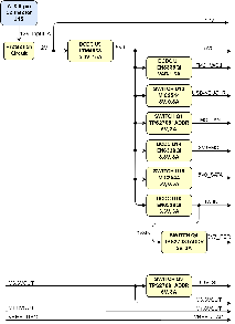 Image Added Image Added
|
|
Power-On Sequence
Power up sequenz is depicted in the following figure. Most of the enables are handled by the SC CPLD and are therefore Firmware dependent. The Power up meets all criteria to power up 4x5 modules.
| Scroll Title |
|---|
| anchor | Figure_PWR_PS |
|---|
| title | Power Sequency |
|---|
|
| Scroll Ignore |
|---|
| draw.io Diagram |
|---|
| border | true |
|---|
| viewerToolbar | true |
|---|
| |
|---|
| fitWindow | false |
|---|
| diagramName | PS_TEF1002 |
|---|
| simpleViewer | false |
|---|
| width | |
|---|
| diagramWidth | 414 |
|---|
| revision | 6 |
|---|
|
|
| Scroll Only |
|---|
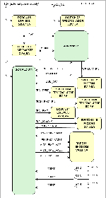 Image Added Image Added
|
|
Power Rails
In the following table power rails acceccible for in or output on any connectors are summarized.
| Scroll Title |
|---|
| anchor | Table_PWR_PR |
|---|
| title | Power Rails |
|---|
|
| Scroll Table Layout |
|---|
| orientation | portrait |
|---|
| sortDirection | ASC |
|---|
| repeatTableHeaders | default |
|---|
| style | |
|---|
| widths | |
|---|
| sortByColumn | 1 |
|---|
| sortEnabled | false |
|---|
| cellHighlighting | true |
|---|
|
| Connector, Pins | Voltage | Direction | Notes |
|---|
| J15, 1,2,3 | 12V | IN | TEF1002 supply voltage | | J16, 1 | 5V | OUT | USB-VBUS_R | | J6, 1 | Depends on 4x5 Module | IN | Directly connected to B2B PSBATT pin | | J2, 2 | 5V | OUT | FMC Fan Connector | | JB1, 10,12 | 1,8V/3.3V | OUT | VCCIOA, selected by J4 | | JB1, 14,16 | 3.3V | OUT | Module supply voltage | | JB1, 40 | 1.8V | IN | Module 1.8V output | | JB1, 80 | Depends on 4x5 Module | OUT | Directly connected to pinheader J6 PSBATT | | JB1, 2,4,6 | 5V | OUT | Module power input | | JB2, 1,3,5,7 | 5V | OUT | Module power input | | JB2, 9,11 | 3.3V | IN | Module 3.3V output | | JB2, 2,4,6,8,10 | 0,8V ... 3.3V | OUT | Module VCCIOB, VCCIOC, VCCIOD connected to FMC VADJ | | JB2, 20 | Depends on 4x5 Module | IN | Module DDR power output | | JB2, 92 | Depends on 4x5 Module | IN | VREF_JTAG | | J13, 1,10 | 3.3V | OUT | FFA supply voltages | | J18, 1,10 | 3.3V | OUT | FFB supply voltages |
|
Power-On Sequence
...
| anchor | Figure_PWR_PS |
|---|
| title | Power Sequency |
|---|
| Scroll Ignore |
|---|
Create DrawIO object here: Attention if you copy from other page, objects are only linked. |
| Scroll Only |
|---|
image link to the generate DrawIO PNG file of this page. This is a workaround until scroll pdf export bug is fixed |
Voltage Monitor Circuit
Power Rails
Bank Voltages
...
| Page properties |
|---|
|
- This section is optional and only for modules.
- use "include page" macro and link to the general B2B connector page of the module series, for example: 4 x 5 SoM LSHM B2B Connectors
| Include Page |
|---|
| PD:4 x 5 SoM LSHM B2B Connectors |
|---|
| PD:4 x 5 SoM LSHM B2B Connectors |
|---|
|
|
...
| Scroll Title |
|---|
| anchor | Table_TS_AMR |
|---|
| title | Module absolute maximum ratings. |
|---|
|
| Scroll Table Layout |
|---|
| orientation | portrait |
|---|
| sortDirection | ASC |
|---|
| repeatTableHeaders | default |
|---|
| style | |
|---|
| widths | |
|---|
| sortByColumn | 1 |
|---|
| sortEnabled | false |
|---|
| cellHighlighting | true |
|---|
|
| Parameter | Min | Max | UnitsReference Document | Reference Document |
|---|
VIN supply voltage | -0.3 | 20 | V | TPS6217 datasheet Note: voltage limitations are not valid for connected FMC module | Storage temperature | -40 | +100 | °C | SML-P11 LED datasheet |
|
Recommended Operating Conditions
| Scroll Title |
|---|
| anchor | Table_TS_AMR |
|---|
| title | Recommended Operating Conditions. |
|---|
|
| Scroll Table Layout |
|---|
| orientation | portrait |
|---|
| sortDirection | ASC |
|---|
| repeatTableHeaders | default |
|---|
| style | |
|---|
| widths | |
|---|
| sortByColumn | 1 |
|---|
| sortEnabled | false |
|---|
| cellHighlighting | true |
|---|
|
| Parameter | Min | Max | Units | Reference Document |
|---|
| VIN supply voltage | 11.4 | 12.6 | V | 12V nominal, ANSI/VITA 57.1 power specification for FMC connector | Board Operating Temperature Range
| 0 | 85 | °C | 10M08SAU169C8G CPLD datasheet |
|
Physical Dimensions
| Scroll Title |
|---|
| anchor | Figure_TS_PD |
|---|
| title | Physical dimensions drawing |
|---|
|
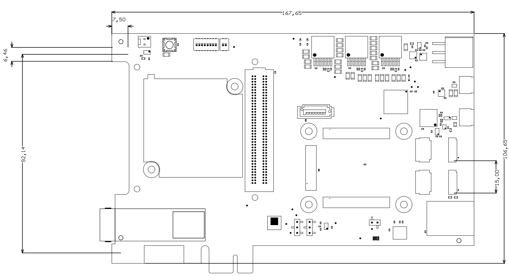 Image Added Image Added |
Variants Currently In Production
...
| Scroll Title |
|---|
| anchor | Table_VCP_SO |
|---|
| title | Trenz Electronic Shop Overview |
|---|
|
| Scroll Table Layout |
|---|
| orientation | portrait |
|---|
| sortDirection | ASC |
|---|
| repeatTableHeaders | default |
|---|
| style | |
|---|
| widths | |
|---|
| sortByColumn | 1 |
|---|
| sortEnabled | false |
|---|
| cellHighlighting | true |
|---|
|
|
...
| Scroll Title |
|---|
| anchor | Figure_RH_HRN |
|---|
| title | Hardware Revision Number |
|---|
|
| draw.io Diagram |
|---|
| border | true |
|---|
| viewerToolbar | true |
|---|
| |
|---|
| fitWindow | false |
|---|
| diagramName | HRN_TEF1002 |
|---|
| simpleViewer | false |
|---|
| width | |
|---|
| diagramWidth | 406 |
|---|
| revision | 1 |
|---|
|
|
Hardware revision number is printed on the PCB board next to the module model number separated by the dash.
...
| Scroll Title |
|---|
| anchor | Table_RH_DCH |
|---|
| title | Document change history. |
|---|
|
| Scroll Table Layout |
|---|
| orientation | portrait |
|---|
| sortDirection | ASC |
|---|
| repeatTableHeaders | default |
|---|
| style | |
|---|
| widths | |
|---|
| sortByColumn | 1 |
|---|
| sortEnabled | false |
|---|
| cellHighlighting | true |
|---|
|
| Date | Revision | Contributor | Description |
|---|
| Page info |
|---|
| infoType | Modified date |
|---|
| dateFormat | yyyy-MM-dd |
|---|
| type | Flat |
|---|
|
| | Page info |
|---|
| infoType | Current version |
|---|
| prefix | v. |
|---|
| type | Flat |
|---|
| showVersions | false |
|---|
|
| | Page info |
|---|
| infoType | Modified by |
|---|
| type | Flat |
|---|
| showVersions | false |
|---|
|
| | -- | all | | Page info |
|---|
| infoType | Modified users |
|---|
| type | Flat |
|---|
| showVersions | false |
|---|
|
| |
|
...