| Scroll Table Layout |
|---|
| orientation | portrait |
|---|
| sortDirection | ASC |
|---|
| repeatTableHeaders | default | style | widths |
|---|
| sortByColumn | 1 |
|---|
| sortEnabled | false |
|---|
| cellHighlighting | true |
|---|
|
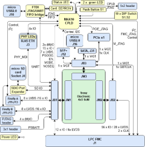
| Signal name | SC CPLD Pin | Connected to | Function | Notes |
|---|
| ACBUS0 | A4 | FTDI U4, pin 22 | GPIO's available to user
| (FIFO or other FTDI functions when FTDI reprogrammed)
| | ACBUS1 | B4 | FTDI U4, pin 23 | | ACBUS2 | A5 | FTDI U4, pin 24 | | ACBUS3 | B5 | FTDI U4, pin 25 | | ACBUS4 | A6 | FTDI U4, pin 26 | | ACBUS5 | B6 | FTDI U4, pin 27 | | ACBUS6 | A7 | FTDI U4, pin 28 | | ACBUS7 | A8 | FTDI U4, pin 29 | | ADBUS4 | A2 | FTDI U4, pin 17 | | ADBUS5 | B2 | FTDI U4, pin 18 | | ADBUS6 | A3 | FTDI U4, pin 19 | | ADBUS7 | B3 | FTDI U4, pin 20 | | TCK | G2 | FTDI U4, pin 12 | Forwarded JTAG signals from FTDI chip.
| (FIFO or other FTDI functions when FTDI reprogrammed)
| | TDI | F5 | FTDI U4, pin 13 | | TDO | F6 | FTDI U4, pin 14 | | TMS | G1 | FTDI U4, pin 15 | | M_TCK | H5 | JB2, pin 100 | 4x5 Module JTAG
| Bank with VCCIO is VREF_JTAG from Module
| | M_TDI | J2 | JB2, pin 96 | | M_TDO | J1 | JB2, pin 98 | | M_TMS | H6 | JB2, pin 94 | | FMC_TCK | F8 | J1, pin D29 | FMC JTAG
| TRST not used
| | FMC_TDI | M7 | J1, pin D30 | | FMC_TDO | N7 | J1, pin D31 | | FMC_TMS | M8 | J1, pin D33 | | FMC_TRST | N8 | J1, pin D34 | | PCIE_TCK | L11 | J3, pin A5 | PCIe JTAG
| Currently not used
| | PCIE_TDI | N12 | J3, pin A6 | | PCIE_TDO | M12 | J3, pin A7 | | PCIE_TMS | M13 | J3, pin A8 | | PCIE_TRST | G10 | J3, pin B9 | | PCIE_PERST | F12 | J3, pin A11 | Indication that PCIe Bus is up (power, clocks) |
| | EN_FMC | L4 | U14, pin 9 | Enable switched 3.3V FMC power | pulled down | | EN_FMC_VADJ | K7 | U1, pin 41 | Enable IO power FMC_VADJ | pulled down | | EN_PER | F13 | Q4, pin 5 | Enable perepherie power 3V3_PER | pulled down | | FAN_FMC_EN | K8 | Q1, pin 5 | Enable FMC FAN |
| | FMC_PG_C2M | M5 | J1, pin D1 | Indicate that all FMC related powers are up | pulled up | | FMC_PRSNT_M2C_L | E9 | J1, pin H2 | Indicate if FMC installed | Low when FMC present | | FMC_SCL | J8 | J1, pin C31 | I2C 2-wire serial bus | MUX in CPLD | | FMC_SDA | F9 | J1, pin C30 | | PG_FMC_VADJ | J6 | U1, pin 35 | Indicate FMC VADJ power is up |
| | FF_RSTL | B9 | J13, pin 6 and J18, pin 6 | Reset configuration | Both FF are resetted simultanously when pulled LOW | | FFA_INTL | E8 | J13, pin 5 | Indicate interrrupt | LOW when fault condition, pulled up | | FFA_MPRS | C10 | J13, pin 3 | Indicate FF Module installed | LOW when Module present, pulled up | | FFA_MSEL | C9 | J13, pin 4 | Select attached FF Module | Pull low to use I2C | | FFA_SCL | D6 | J13, pin 8 | I2C 2-wire serial bus | MUX in CPLD | | FFA_SDA | E6 | J13, pin 7 | | FFB_INTL | A10 | J18, pin 5 | Indicate interrrupt | LOW when fault condition, pulled up | | FFB_MPRS | A11 | J18, pin 3 | Indicate FF Module installed | LOW when Module present, pulled up | | FFB_MSEL | B10 | J18, pin 4 | Select attached FF Module | Pull low to use I2C | | FFB_SCL | D8 | J18, pin 8 | I2C 2-wire serial bus | MUX in CPLD | | FFB_SDA | A9 | J18, pin 7 | | CPLD_IO_1 | B12 | JB1, pin 88 | (M)IOs from 4x5 Module | (M)IOs used for ETH PHY LEDs
| | CPLD_IO_2 | A12 | JB1, pin 92 | (M)IOs from 4x5 Module | | M10_RST | D1 | TP22 |
| Not used
| | M10_RX | E4 | TP24 | | M10_TX | E3 | TP23 | | EN1 | D11 | JB1, pin 27 | Enable on module power | Depends on module, on some similar to reset. | | MODE | B11 | JB1, pin 31 | Boot Mode selection | For Zynq modules only. (LOW → SD, HIGH → primary QSPI) | | NOSEQ | E13 | JB1, pin 8 | Disable module CPLD power management | Depends on module. On some modules no extended CPLD power management avaialble. | | PGOOD | C11 | JB1, pin 29 | Power good signal | This is only for monitoring, do not use as powerenable! Pulled up. | | RESIN | E12 | JB2, pin 17 | Module Reset | Aktive LOW | | M3.3VOUT | M4 | JB2, pin 9 and 11 | Indicates module power is up | Used for perepherie power enable. | | SFPA_LOS | M10 | J12, pin 8 | SFP signal loss | HIGH indicates signal loss | | SFPA_M-DEF0 | F10 | J12, pin 6 | SFP modul absent | HIGH when module physically absent | | SFPA_RS0 | N10 | J12, pin 7 | SFP rate select RX | LOW for 1000BASE-SX, HIGH for 10GBASE-SR | | SFPA_RS1 | M11 | J12, pin 9 | SFP rate select TX | LOW for 1000BASE-SX, HIGH for 10GBASE-SR | | SFPA_SCL | L10 | J12, pin 5 | I2C 2-wire serial bus | MUX in CPLD | | SFPA_SDA | N9 | J12, pin 4 | | SFPA_TX_DIS | M9 | J12, pin 3 | SFP transmitter disable | HIGH disables transmitter | | SFPA_TX_FAULT | G9 | J12, pin 2 | Indicates SFP laser fault | HIGH indicates fault | | VID0_FMC_VADJ | E10 | U1, pin 34 | FMC_VADJ Voltage select | Chip internal pulled up
| | VID1_FMC_VADJ | J7 | U1, pin 33 | | VID2_FMC_VADJ | L5 | U1, pin 32 | | VID0 | K6 | S2-1 | For FMC_VADJ Voltage select
|
| | VID1 | N5 | S2-2 | | VID2 | N4 | S2-3 | | JTAGEN | E5 | S2-4 |
|
| | FMC_JTAG | L3 | S2-6 |
|
| | CM0 | M3 | S2-7 |
|
| | CM1 | L2 | S2-8 |
|
| | CM2 | K2 | S3-1 |
|
| | USR0 | K1 | S3-2 |
|
| | USB_OC | D9 | U12, pin 5 |
|
| | BUTTON | N6 | S1 |
|
| | LED1 | J5 | D1 | user LED |
| | LED2 | K5 | D2 | | - | C2 | D4 | Status LED | For further explanation see SC CPLD Firmware description | | PHY_LED1 | D12 | J9 | Phy LEDs
|
| | PHY_LED1R | C13 | J9 | | PHY_LED2 | B13 | J9 | | PHY_LED2R | C12 | J9 | | A_00_N | J10 | JB1, pin 38 | Module to CPLD communication
| Currently "three wire" I2C and RGPIO, see SC CPLD Firmware description
| | A_00_P | K10 | JB1, pin 36 | | A_01_N | L12 | JB1, pin 35 | | A_01_P | K11 | JB1, pin 37 | | A_02_N | J12 | JB1, pin 41 | | A_02_P | K12 | JB1, pin 39 | | A_03_N | H10 | JB1, pin 44 | | A_03_P | J9 | JB1, pin 42 | | A_04_N | H13 | JB1, pin 47 | | A_04_P | J13 | JB1, pin 45 | | A_05_N | H8 | JB1, pin 57 | | A_05_P | H9 | JB1, pin 55 | | A_06_N | G12 | JB1, pin 49 | | A_06_P | G13 | JB1, pin 51 | | A_07 | L13 | JB1, pin 34 |
|