Page History
| Page properties | ||||
|---|---|---|---|---|
| ||||
In this section you must explain how to power on the board and run the Reference Design (test board) on the particular module. The main points must be mentioned are:
|
| Scroll pdf ignore | |
|---|---|
Table of Contents
|
TEF1002
Overview
| Scroll Title | |||||||||||||||||||||||||||||||||||||||||||||||||||||||||||
|---|---|---|---|---|---|---|---|---|---|---|---|---|---|---|---|---|---|---|---|---|---|---|---|---|---|---|---|---|---|---|---|---|---|---|---|---|---|---|---|---|---|---|---|---|---|---|---|---|---|---|---|---|---|---|---|---|---|---|---|
| |||||||||||||||||||||||||||||||||||||||||||||||||||||||||||
|
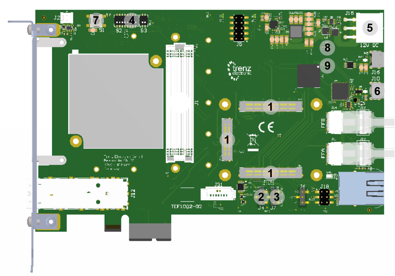
- 4x5 module connectors
- Jumper J4 (VCCIOA)
- Jumper J7 (VCCA_SD)
- Dip swiches S2 and S3
- 6-pin ATX Power Connector
- micro USB connector for FTDI USB to JTAG/UART bridge
- Push button
- Power LED
- Status LED
- top load microSD card cageAttache 4x5 module to TEF1002
- Select Voltage VCCA_SD of 4x5 module bank where SD-Card is connected by Jumper J7 (1-2 →3.3V; 2-3 1.8V). Compare TRM of actually used 4x5 module.
- Select VCCIOA Voltage by setting J4 (1-2 →3.3V; 2-3 1.8V). If both FFA and FFB are not used any setting is ok. Do not leave open (communication of 4x5 module with TEF1002 CPLD is only possible with availabe VCCIOA)!
Select dip switch settings according to the attached 4x5 module and your needs:
Dip Setting Note S1-1
OFF FMC _VADJ OFF. The choice OFF, ON, OFF selects 1.8V FMC_VADJ, wich is a valid bank power for TE0720.
S1-2 OFF S1-3 OFF S1-4 ON Selects 4x5 module SOC/FPGA JTAG S1-5 ON S1-6 OFF S1-7 ON Module power enable. S1-8 ON Use extended power sequenzing. S2-1 OFF/ON For Zynq modules: Primary Boot Mode SD/QSPI. S2-2 OFF ON for TE0720 (overide automatic enable FMC__VADJ). For TE0720 bank bank 34 has to be powerded to start up. Therefore FMC VADJ has to be set to a valid value e.g. 1.8V - Connect 12V ATX connector
- Connect mico USB J10 to PC
- Use Xilinx JTAG tools to programm FPGA or for Zynq modules use micro SD Card.
- Use e.g. Putty on PC to check for UART interactions.
...
| hidden | true |
|---|---|
| id | Comments |
In this section you must explain how to power on the board and run the Reference Design (test board) on the particular module. The main points must be mentioned are:
...
Explain the UART connection
Refer to the Reference Design
...
- .
| Scroll pdf ignore | |
|---|---|
Table of Contents
|
TExxxx with TExxxx
Overview
...
| anchor | Figure_Overview |
|---|---|
| title | Board Overview |
...
| scroll-pdf | true |
|---|---|
| scroll-office | true |
| scroll-chm | true |
| scroll-docbook | true |
| scroll-eclipsehelp | true |
| scroll-epub | true |
| scroll-html | true |
...
Power supply
| Page properties | ||||
|---|---|---|---|---|
| ||||
The input power supply must be mentioned. |
Single ??V 12V power supply with minimum current capability of ??A 3A is recommended to power on the board.
...
Overview
Content Tools