...
| Scroll Title |
|---|
| anchor | Figure_Overview |
|---|
| title | Board Overview |
|---|
|
| Scroll Ignore |
|---|
| scroll-pdf | true |
|---|
| scroll-office | true |
|---|
| scroll-chm | true |
|---|
| scroll-docbook | true |
|---|
| scroll-eclipsehelp | true |
|---|
| scroll-epub | true |
|---|
| scroll-html | true |
|---|
| | draw.io Diagram |
|---|
| border | true |
|---|
| viewerToolbar | true |
|---|
| |
|---|
| fitWindow | false |
|---|
| diagramName | TEF1002 Overview |
|---|
| simpleViewer | false |
|---|
| width | |
|---|
| diagramWidth | 641 |
|---|
| revision | 2 |
|---|
|
| draw.io Diagram |
|---|
| border | true |
|---|
| viewerToolbar | true |
|---|
| |
|---|
| fitWindow | false |
|---|
| diagramName | TEF1002_Overview_bottom |
|---|
| simpleViewer | false |
|---|
| width | |
|---|
| diagramWidth | 635 |
|---|
| revision | 2 |
|---|
|
|
| Scroll Only |
|---|
|
|
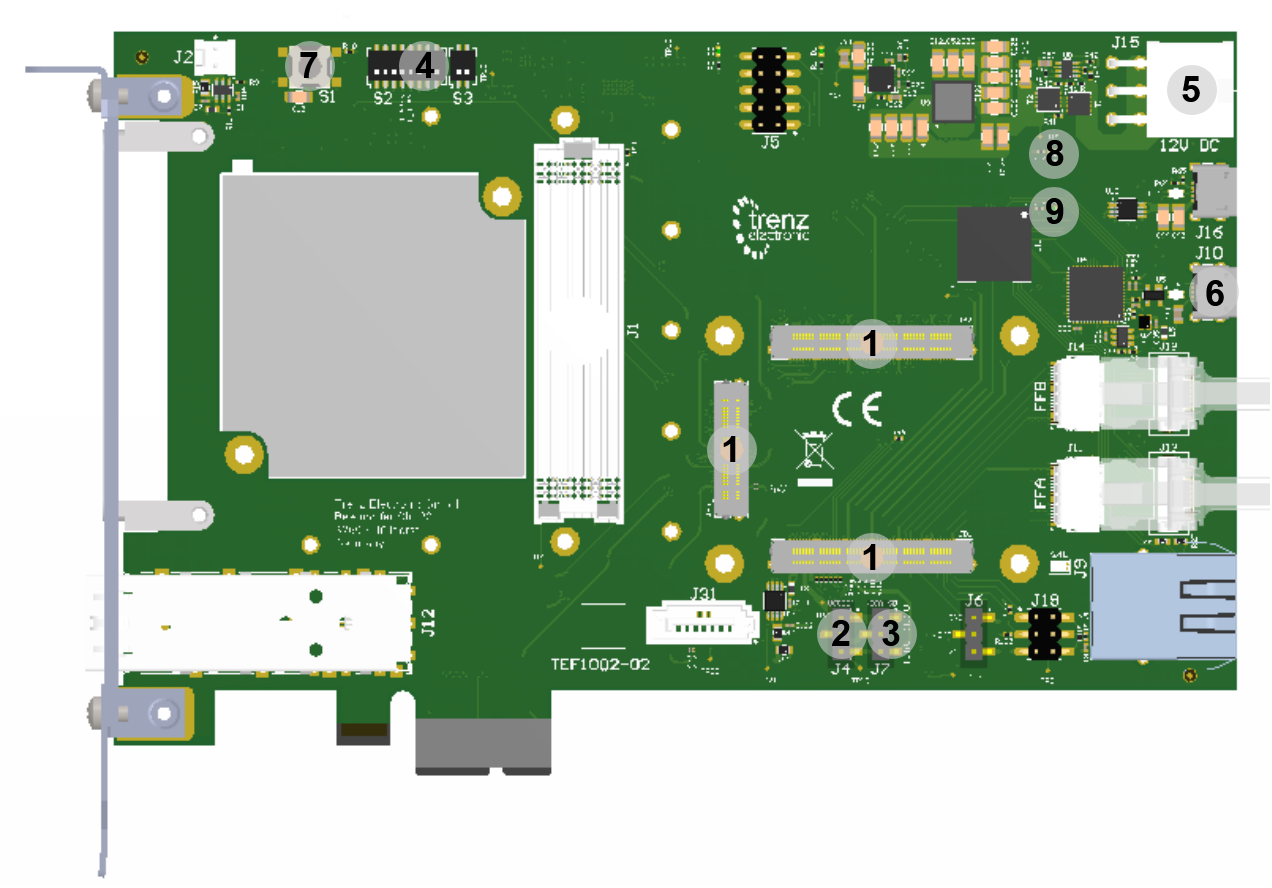
- 4x5 module connectors
- Jumper J4 (VCCIOA)
- Jumper J7 (VCCA_SD)
- Dip swiches S2 and S3
- 6-pin PCI-E ATX Power Connector
- micro USB connector for FTDI USB to JTAG/UART bridge
- Push button
- Power LED
- Status LED
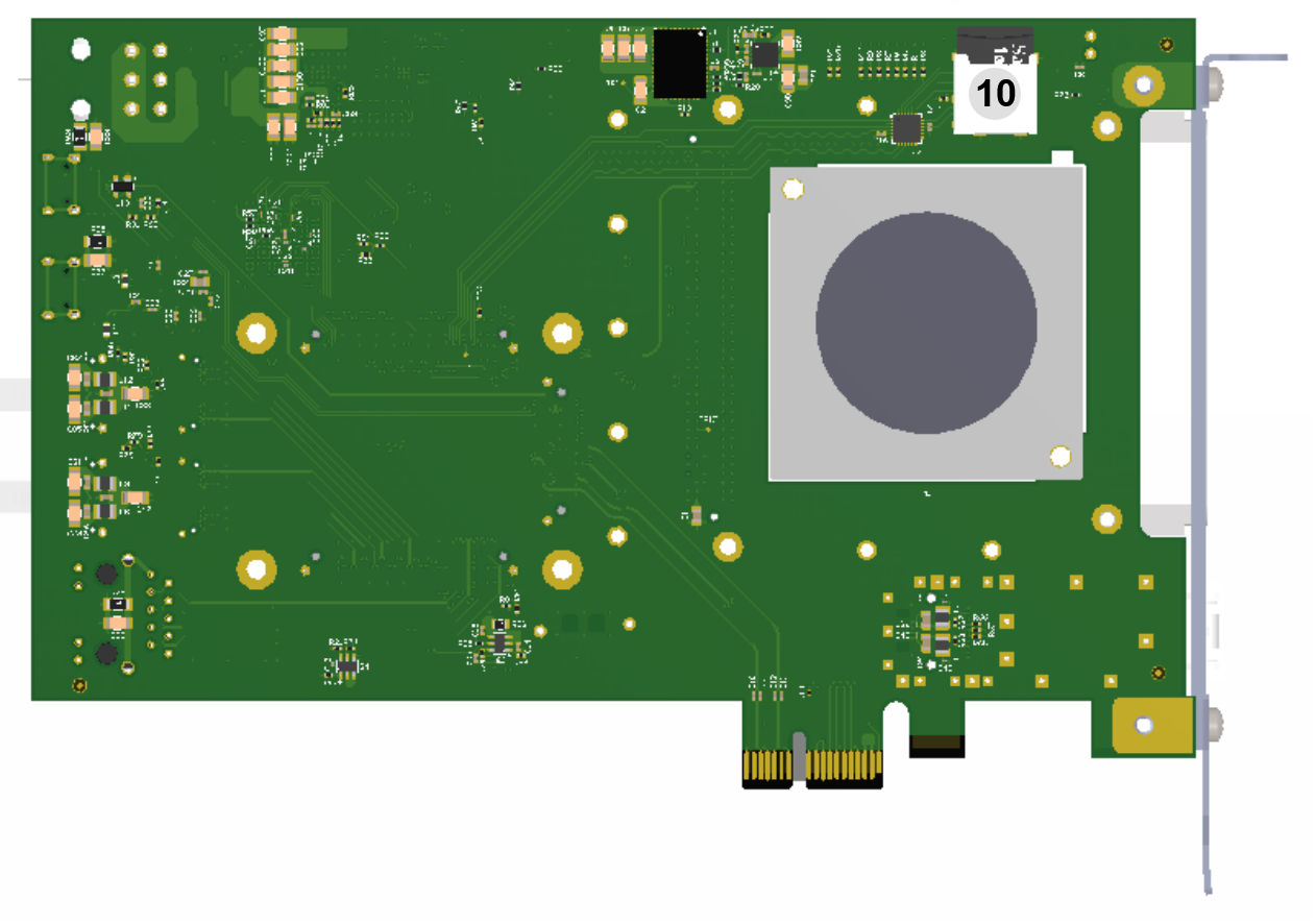
- top load microSD card cage
- Select Voltage VCCA_SD of 4x5 module bank where SD-Card is connected by Jumper J7 (1-2 →3.3V; 2-3 1.8V). Compare TRM of actually used 4x5 module.
Select VCCIOA Voltage by setting J4 (1-2 →3.3V; 2-3 1.8V). If both FFA and FFB are not used any setting is ok. Do not leave open (communication of 4x5 module with TEF1002 CPLD is only possible with availabe VCCIOA)!
Power supply
| Page properties |
|---|
|
The input power supply must be mentioned. |
Single 12V power supply with minimum current capability of 3A is recommended to power on the board via the 6-pin PCI-E ATX connector.
DIP-Switches and Push Buttons
| Page properties |
|---|
|
Explain all DIP switches functionality. |
Select dip switch settings according to the attached 4x5 module and your needs. Compare Dip switch setting with TRM of your module and table in TRM of TEF1002. Following a general configuration is shown.
| Scroll Title |
|---|
| anchor | Table_DIP_PB |
|---|
| title | DIP Switches /Push Buttons |
|---|
|
| Scroll Table Layout |
|---|
| orientation | portrait |
|---|
| sortDirection | ASC |
|---|
| repeatTableHeaders | default |
|---|
| style | |
|---|
| widths | |
|---|
| sortByColumn | 1 |
|---|
| sortEnabled | false |
|---|
| cellHighlighting | true |
|---|
|
| Dip | Setting | Note |
|---|
| S1 |
| Push button configured by CPLD as reset | S2-1 | OFF | OFF, OFF, OFF selects FMC _VADJ OFF. The choice OFF, ON, OFF selects 1.8V FMC_VADJ, |
|
...
which is a valid bank power for TE0720.
| | S2-2 | OFF | | S2-3 | OFF | | S2-4 | ON | Selects 4x5 module SOC/FPGA JTAG | | S2-5 | ON | | S2-6 | OFF | | S2-7 | ON | Module power enable. | | S2-8 | ON | Use extended power sequenzing. | | S3-1 | OFF/ON | For Zynq modules: Primary Boot Mode SD/QSPI. | | S3-2 | OFF | ON for TE0720 (overide automatic enable FMC_ |
|
...
| VADJ). For TE0720 bank bank 34 has to be powerded to start up. Therefore FMC VADJ has to be set to a valid value e.g. 1.8V |
|
...
Jumpers
Power supply
| Page properties |
|---|
|
The input power supply must be mentioned. |
Single 12V power supply with minimum current capability of 3A is recommended to power on the board via the 6-pin PCI-E ATX connector.
DIP-Switches and Push Buttons
| Page properties |
|---|
|
Explain all DIP switches functionality. |
Select dip switch settings according to the attached 4x5 module and your needs.
Explain all Jumpers functionality and connection. |
For Jumper J7 compare TRM of actually used 4x5 module. The voltage of the bank where the SDIO signals are connected has to selected. J4 selects the module bank voltage VCCIOA. It has to be selected in accordance with IO voltage of signals connected to FFA and FFB. If both FFA and FFB are not used any setting is ok. Do not leave open (communication of 4x5 module with TEF1002 CPLD is only possible with availabe VCCIOA)!Compare Dip switch setting with TRM of your module and table in TRM of TEF1002
| Scroll Title |
|---|
| anchor | Table_DIP_PBJumpers |
|---|
| title | DIP Switches /Push ButtonsJumpers |
|---|
|
| Scroll Table Layout |
|---|
| orientation | portrait |
|---|
| sortDirection | ASC |
|---|
| repeatTableHeaders | default |
|---|
| style | |
|---|
| widths | |
|---|
| sortByColumn | 1 |
|---|
| sortEnabled | false |
|---|
| cellHighlighting | true |
|---|
|
Signal| Designator | B2B | Active Level | |
Jumpers
| Page properties |
|---|
|
Explain all Jumpers functionality and connection. |
...
| anchor | Table_Jumpers |
|---|
| title | Jumpers |
|---|
| Power Rail | 3.3V | 1.8V | Remark |
|---|
| J7 | VCCA_SD | 1-2 | 2-3 | Powers SDIO Levelshifter on 4x5 module side. | | J4 | VCCIOA | 1-2 | 2-3 | Powers 4x5 bank, where FFA and FFB high speed signals are connected. |
|
...
LEDs
| Page properties |
|---|
|
Explain all user LEDs functionality and connections. |
There are three user LEDs which can be used for variant purposesfour LEDs on the board. Compare corresponding table in TEF1002 TRM.
| Scroll Title |
|---|
| anchor | Table_LED |
|---|
| title | Carrier LEDs |
|---|
|
| anchor | Table_| Scroll Table Layout |
|---|
| orientation | portrait |
|---|
| sortDirection | ASC |
|---|
| repeatTableHeaders | default |
|---|
| style | |
|---|
| widths | |
|---|
| sortByColumn | 1 |
|---|
| sortEnabled | false |
|---|
| cellHighlighting | true |
|---|
|
|
|---|
| Designator | Color | Connected to | B2B | Active Level | Note |
|---|
| Scroll Title |
|---|
| | _Module
| title | Module LEDs |
|---|
scroll-tablelayout | widths | | sortByColumn | 1 |
|---|
| sortEnabled | false |
|---|
| cellHighlighting | true |
|---|
| orientation | portrait |
|---|
| sortDirection | ASC |
|---|
| repeatTableHeaders | default |
|---|
style | scroll-title |
| anchor | Table_LED_Carrier |
|---|
| title | Carrier LEDs |
|---|
|
| 3V3IN | Power | ON when 3.3V generated from 12V input is up | | D4 | SC CPLD U11, Pin C2 | Status | SC CPLD firmware dependent, for further description see firmware description. |
| Scroll Table Layout |
|---|
|
| orientation | portrait |
|---|
| sortDirection | ASC |
|---|
| repeatTableHeaders | default |
|---|
style | widths | | sortByColumn | 1 |
|---|
| sortEnabled | false |
|---|
| cellHighlighting | true |
|---|
| Designator | Color | Connected to | Active Level | Note
JTAG/UART
| Page properties |
|---|
|
Explain JTAG or UART connection breifly. |
JTAG and UART connections are available through mini USB connector.JTAG(first FTDI port) and UART(second FTDI port) is over MicroUSB connector possibleavailable. External JTAG Programmer is not needed.
...
...
Connected to
...
B2B Pin
...
Reference Designs
| Page properties |
|---|
|
In this Section you must refer to the Reference Design (Test board) for the particular module. For Example: TE0728 Reference Designs |
Notes
...
| Page properties |
|---|
|
In this Section you must refer to the Resources Page for the particular module. For Example: TE0728 Resources |
...