Page History
...
...
| HTML |
|---|
<!-- tables have all same width (web max 1200px and pdf full page(640px), flexible width or fix width on menu for single column can be used as before) -->
<style>
.wrapped{
  width: 100% !important;
  max-width: 1200px !important;
 }
</style> |
...
| hidden | true |
|---|---|
| id | Comments |
Important General Note:
...
Designate all graphics and pictures with a number and a description, Use "Scroll Title" macro
...
Figure template:
...
| anchor | Figure_anchorname |
|---|---|
| title | Text |
| Scroll Ignore |
|---|
Create DrawIO object here: Attention if you copy from other page, objects are only linked. |
| Scroll Only |
|---|
image link to the generate DrawIO PNG file of this page. This is a workaround until scroll pdf export bug is fixed |
...
Table template:
- Layout macro can be use for landscape of large tables
...
| anchor | Table_tablename |
|---|---|
| title | Text |
...
The anchors of the Scroll Title should be named consistant across TRMs. A incomplete list of examples is given below
<type>_<main section>_<name>
- type: Figure, Table
- main section:
- "OV" for Overview
- "SIP" for Signal Interfaces and Pins,
- "OBP" for On board Peripherals,
- "PWR" for Power and Power-On Sequence,
- "B2B" for Board to Board Connector,
- "TS" for Technical Specification
- "VCP" for Variants Currently in Production
- "RH" for Revision History
- name: custom, some fix names, see below
- Fix names:
"Figure_OV_BD" for Block Diagram
"Figure_OV_MC" for Main Components
"Table_OV_IDS" for Initial Delivery State
"Table_PWR_PC" for Power Consumption
- "Figure_PWR_PD" for Power Distribution
- "Figure_PWR_PS" for Power Sequence
- "Figure_PWR_PM" for Power Monitoring
- "Table_PWR_PR" for Power Rails
- "Table_PWR_BV" for Bank Voltages
"Table_TS_AMR" for Absolute_Maximum_Ratings
"Table_TS_ROC" for Recommended_Operating_Conditions
- "Figure_TS_PD" for Physical_Dimensions
- "Table_VCP_SO" for TE_Shop_Overview
"Table_RH_HRH" for Hardware_Revision_History
- "Figure_RH_HRN" for Hardware_Revision_Number
- "Table_RH_DCH" for Document_Change_History
...
| Page properties | ||||
|---|---|---|---|---|
| ||||
----------------------------------------------------------------------- |
| Page properties | ||||
|---|---|---|---|---|
| ||||
Note for Download Link of the Scroll ignore macro:
|
| Scroll Ignore |
|---|
| Scroll pdf ignore | |
|---|---|
Table of Contents
|
Overview
The Trenz Electronic TE0022-01 board is an industrial-grade SoC module based on Intel Cyclone V FPGA, an ethernet PHY, one GByte DDR3 SDRAM and one 32 MByte Quad SPI Flash memory for configuration and operation per HPS and FPGA, and powerful switching-mode power supplies for all on-board voltages.
...
Notes :
...
Short Link of the wiki resources reference:
...
Use short link the Wiki Resource page, for example: http://trenz.org/te0728-info
...
...
...
Key Features
...
| hidden | true |
|---|---|
| id | Comments |
Note:
'description: Important components and connector or other Features of the module
→ please sort and indicate assembly options
Key Features' must be split into 6 main groups for modues:
- SoC/FPGA
- Package:
- Speed:
- Temperature:
- RAM/Storage
- E.g. SDRAM, SPI
- On Board
- E.g. CPLD, PLL
- Interface
- E.g. ETH, USB, B2B, Display port
- Power
- E.g. Input supply voltage
- Dimension
Key Features' must be split into 6 main groups for carrier:
...
- TE0808, TE807, TE0803,...
...
- E.g. SDRAM, SPI
...
- E.g. CPLD, PLL
...
- E.g. ETH, USB, B2B, Display port
...
- E.g. Input supply voltage
...
...
...
...
...
...
...
...
...
Create DrawIO object here: Attention if you copy from other page, objects are only linked.
...
|
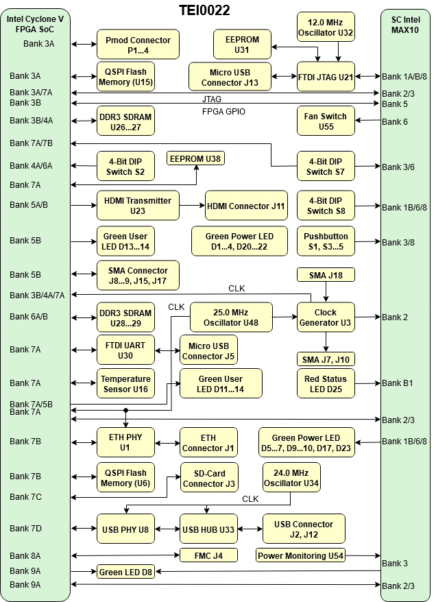
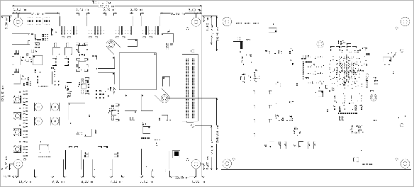
Main Components
| Page properties | ||||
|---|---|---|---|---|
| ||||
Notes :
|
| Scroll Title | |||
|---|---|---|---|
|
...
...
Create DrawIO object here: Attention if you copy from other page, objects are only linked.
| Scroll Only |
|---|
image link to the generate DrawIO PNG file of this page. This is a workaround until scroll pdf export bug is fixed |
- ...
- ...
- ...
Initial Delivery State
| Page properties | ||||
|---|---|---|---|---|
| ||||
Notes : Only components like EEPROM, QSPI flash can be initialized by default at manufacture. If there is no components which might have initial data ( possible on carrier) you must keep the table empty |
...
| anchor | Table_OV_IDS |
|---|---|
| title | Initial delivery state of programmable devices on the module |
...
Storage device name
...
Content
...
Notes
...
HPS SPI Flash
...
HPS Configuration
...
Ethernet MAC
...
Configuration Signals
| Page properties | ||||
|---|---|---|---|---|
| ||||
|
|
- Intel Cyclone V, U10
- DDR3 SDRAM, U26...27
- DDR3 SDRAM, U28...29
- FMC, J4
- Pmod, P1...4
- SD Card Connector, J3
- Ethernet PHY, U1
- RJ45 Connector, J1
- USB PHY, U8
- USB HUB, U33
- USB Connector, J2, J12
- HDMI Transmitter, U23
- HDMI Connector, J11
- Intel MAX10, U41
- Micro USB to UART Interface, J5, U30
- USB to JTAG , U21
- Micro USB JTAG and UART, J13
- SMA Connector
- Push Button, S1, S3...5
- LED
- 4-Bit DIP Switch, S2, S7...8
- 12 V Power Jack, J6
- Clock Generator, U48
- Programmable Clock Generator, U3
- QSPI - FPGA PS, U6
- QSPI - FPGA PL, U15
- Temperature Sensor, U16
- EEPROM, U38
Initial Delivery State
| Page properties | ||||
|---|---|---|---|---|
| ||||
|
...
...
...
BOOTSEL[1..0] Signal State
...
00
...
FPGA
...
| anchor | Table_OV_RST |
|---|---|
| title | Reset process. |
...
Reset
...
HPS cold reset
...
Signals, Interfaces and Pins
| Page properties | ||||
|---|---|---|---|---|
| ||||
Notes :
|
FMC LPC Connector
The FMC (FPGA Mezzanine Card) connector J4 with low pin count (LPC) provides as an ANSI/VITA 57.1 standard a modular interface to the Intel Cyclone V FPGA and exposes numerous of its I/O pins for use by other mezzanine modules and expansion cards.
The connector supports single ended (VCCIO: FMC_VADJ) and differential signaling as the I/O's are routed from the FPGA banks as LVDS-pairs to the FMC connector.
...
| anchor | Table_SIP_FMC |
|---|---|
| title | FMC connectors information |
...
The FMC connector provides further interfaces like JTAG and I²C interfaces:
...
| anchor | Table_SIP_FMC_Interfaces |
|---|---|
| title | FMC connector pin-outs of available interfaces |
...
FMC_TCK, Pin J4-D29
FMC_TMS, Pin J4-D33
FMC_TDI, Pin J4-D30
FMC_TDO, Pin J4- D31
FMC_TRST#, Pin J4- D34
...
FMC_SCL, Pin J4-C30
FMC_SDA, Pin J4-C31
...
FMC_PRSNT_M2C#, Pin J4-H2 (pulled-up to +3.3V)
FMC_PG_C2M, Pin J4-D1 (pulled-up to +3.3V)
...
'PG' = 'Power Good'-signal
'C2M' = carrier to (Mezzanine) module
'M2C' = (Mezzanine) module to carrier
...
...
...
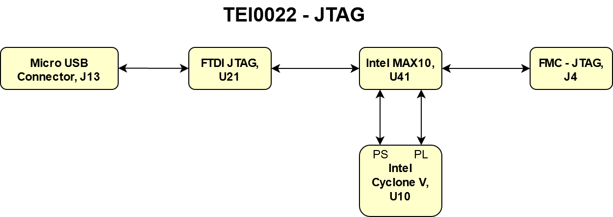
JTAG Interface
According to the JTAGEN and JTAGSEL[1..0] pins the management Intel MAX10, the Intel Cyclone V HPS, the Intel Cyclone V FPGA or the FMC can be accessed.
...
| anchor | Table_SIP_JTG |
|---|---|
| title | JTAG pins connection |
...
JTAGSEL1
...
JTAGSEL1
...
On-board Peripherals
| Page properties | ||||
|---|---|---|---|---|
| ||||
Notes :
|
| Page properties | ||||
|---|---|---|---|---|
| ||||
Notes : In the on-board peripheral table "chip/Interface" must be linked to the corresponding chapter or subsection |
...
| anchor | Table_OBP |
|---|---|
| title | On board peripherals |
...
...
...
Temperatur Sensor
The temperature sensor ADT7410 is implemented on the TEI0022 board.
Quad SPI Flash Memory
| Page properties | ||||
|---|---|---|---|---|
| ||||
Notes : Minimum and Maximum density of quad SPI flash must be mentioned for other assembly options. |
Two 256 Mbit (32 MByte) Quad SPI Flash Memory (Micron MT25QL256ABA8E12, U6, U15) are provided for FPGA and HPS configuration file storage. After configuration process completes the remaining free memory can be used for application data storage. All four SPI data lines are connected to the FPGA and the HPS allowing x1, x2 or x4 data bus widths to be used. The maximum data transfer rate depends on the bus width and clock frequency.
Quad SPI Flash memory U6 is connected to the HPS bank 7B and U15 to FPGA bank 3A.
...
| anchor | Table_OBP_QSPI_HPS |
|---|---|
| title | HPS Quad SPI interface signals and connections |
...
...
| anchor | Table_OBP_QSPI_FPGA |
|---|---|
| title | FPGA Quad SPI interface signals and connections |
...
Programmable Clock Generator
...
...
...
...
...
...
...
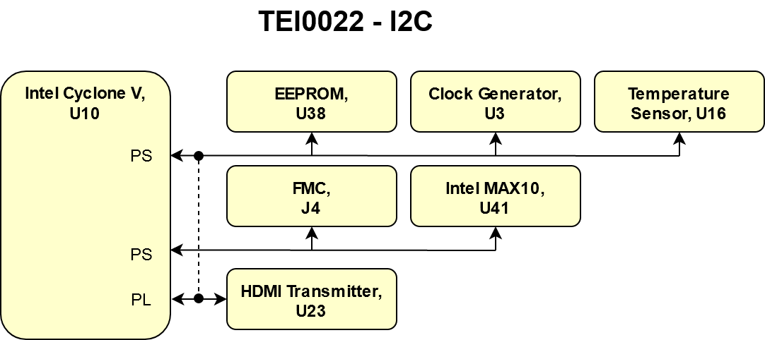
I2C
The TEI0022 provides two independent I2C busses. One bus is used to connect the FMC I2C with the Intel Cyclone V HPS. The other bus is used to handle the on-board I2C devices.
...
| anchor | Table_OBP_I2C |
|---|---|
| title | On-board peripherals' I2C-interfaces device slave addresses |
...
...
IN1
...
-
...
Not used
...
IN3
...
Reference input clock
...
IN4
...
IN5
...
-
...
I²C interface muxed to FPGA
Slave address: 0x70.
...
I²C interface muxed to FPGA
Slave address: 0x70.
...
CLK0A/B
...
CLK_B3B_p/n
...
Clock to FPGA bank 3B
...
CLK1A/B
...
CLK_B4A_p/n
...
Clock to FPGA bank 4A
...
Clock to Intel MAX10 bank 2
...
Oscillators
The FPGA module has following reference clocking source provided by an on-board oscillator:
...
| anchor | Table_OBP_OSC |
|---|---|
| title | Reference clock signals |
...
...
System Controller Intel MAX10
The TEI0022 is equipped with an Intel MAX10 (U41) which is the central system management unit where essential control signals are logically linked by the implemented logic of the FPGA firmware. This generates output signals to control the system, the on-board peripherals and the interfaces. Interfaces like JTAG and buttons between the on-board peripherals and to the FPGA-module are by-passed, forwarded and controlled by the System Controller. Other tasks of the System Controller are the monitoring of the power-on sequence and configuration of the Intel Cyclone V FPGA. The functionalities and configuration of the pins depend on its firmware.
EEPROM
The TEI0022 board contains two EEPROMs for configuration and general user purposes.
...
| anchor | Table_OBP_EEPROM |
|---|---|
| title | On-board configuration EEPROMs overview |
...
High-Speed USB ULPI PHY
USB PHY (U8) is provided by USB3320C from Microchip. The ULPI interface is connected to the Intel Cyclone V HPS. I/O voltage is fixed at 3.3 V and PHY reference clock input is supplied from the on-board 24.0 MHz oscillator (U34).
...
| anchor | Table_OBP_USB_PHY |
|---|---|
| title | USB PHY interface connections |
...
4-Port USB 2.0 Hub
On the TEI0022 board there are up to four USB 2.0 Hi-Speed ports available. The USB 2.0 ports are provided by Microchip Cypress USB2514B 4-port USB 2.0 Hub controller (U33) which is connected to the USB PHY USB3320C (U8) connected to the Intel Cyclone V HPS via ULPI.
Buttons
...
| ||||||||||||||||||||||||||||
| Scroll Title | ||||||||||||||||||||||||||||||||
|---|---|---|---|---|---|---|---|---|---|---|---|---|---|---|---|---|---|---|---|---|---|---|---|---|---|---|---|---|---|---|---|---|
| ||||||||||||||||||||||||||||||||
|
Micro USB Connector (UART)
| Anchor | ||||
|---|---|---|---|---|
|
A UART connection between the USB B connector J5 and the Intel Cyclone HPS U10 is possible via the FT234XD (U30) chip.
USB Connector
On the TEI0022 board there are up to four USB 2.0 Hi-Speed ports available (J2, J12).
HDMI Connector
The TEI0022 provides an HDMI Connector J11.
SD Card Connector
SD Card connector J3 is connected to the Intel Cyclone V U10.
RJ45 Connector
The board TEI0022 provides an ethernet interface via the RJ45 connector J1.
I2C
The TEI0022 provides three independent I2C busses. One bus is used to connect the FMC I2C with the Intel Cyclone V HPS. The second bus is used to connect the HDMI device to the Intel Cyclone V FPGA. The third bus is used to handle the other on-board I2C devices. Via assembly option, it is possible to connect bus two to bus three.
| Scroll Title | ||||||||||||||||||||||||||||||||||||||||||||||||||||||
|---|---|---|---|---|---|---|---|---|---|---|---|---|---|---|---|---|---|---|---|---|---|---|---|---|---|---|---|---|---|---|---|---|---|---|---|---|---|---|---|---|---|---|---|---|---|---|---|---|---|---|---|---|---|---|
| ||||||||||||||||||||||||||||||||||||||||||||||||||||||
|
| Scroll Title | ||||||||||||||||||||||||||||||||
|---|---|---|---|---|---|---|---|---|---|---|---|---|---|---|---|---|---|---|---|---|---|---|---|---|---|---|---|---|---|---|---|---|
| ||||||||||||||||||||||||||||||||
|
On-board Peripherals
| Scroll Ignore | ||||||||||||||||
|---|---|---|---|---|---|---|---|---|---|---|---|---|---|---|---|---|
| ||||||||||||||||
| Page properties | ||||||||
|---|---|---|---|---|---|---|---|---|
| ||||||||
Notes : In the on-board peripheral table "chip/Interface" must be linked to the corresponding chapter or subsection by assigning advance link using: #NameOfTheSection Example:
|
| Page properties | ||||
|---|---|---|---|---|
| ||||
For example subsections see: <Series Name> TRM Template section examples#%3CSeriesName%3ETRMTemplatesectionexamples-On-boardPeripherals |
| Scroll Title | |||||||||||||||||||||||||||||||||||||||||||||||||||||||||||||||||||||||||||
|---|---|---|---|---|---|---|---|---|---|---|---|---|---|---|---|---|---|---|---|---|---|---|---|---|---|---|---|---|---|---|---|---|---|---|---|---|---|---|---|---|---|---|---|---|---|---|---|---|---|---|---|---|---|---|---|---|---|---|---|---|---|---|---|---|---|---|---|---|---|---|---|---|---|---|---|
| |||||||||||||||||||||||||||||||||||||||||||||||||||||||||||||||||||||||||||
|
System Controller Intel MAX 10
The TEI0022 is equipped with an Intel MAX 10 (U41) which is the central system management unit where essential control signals are logically linked by the implemented logic of the FPGA firmware. This generates output signals to control the system, the on-board peripherals and the interfaces. Interfaces like JTAG are by-passed, forwarded and controlled by the System Controller. Other tasks of the System Controller are the monitoring of the power-on sequence and configuration of the Intel Cyclone V FPGA. The functionalities and configuration of the pins depend on its firmware.
Intel Cyclone V
The Intel Cyclone V device used at the TEI0022 board is a SoC with integrated ARM-based HPS. The 5CSEMA5F31C8N version delivers one hard memory controller, 80K logic elements in an FineLineBGA (FBGA) with 896 pins for the commercial temperature range of TJ = 0...85 °C with speed grade eight.
DDR3 SDRAM
| Page properties | ||||
|---|---|---|---|---|
| ||||
Notes : Minimum and Maximum density of DDR3 SDRAM must be mentioned for other assembly options. (pay attention to supported address length for DDR3) |
The TEI0022 SoM has one GByte volatile DDR3 SDRAM memory per FPGA (U26, U27) and HPS (U28, U29) for storing user application code and data.
- Part number: IS43TR16256BL-125KBLI
- Supply voltage: 1.5 V
- Speed: TBD
- Temperature: TC = -40 °C up to 95 °C
Gigabit Ethernet PHY
On-board Gigabit Ethernet PHY (U1) is provided with Analog Devices ADIN1300. The Ethernet PHY RGMII interface is connected to the Intel Cyclone V HPS. I/O voltage is fixed at 3.3 V. The reference clock input of the PHY is supplied from the on-board 25.0 MHz oscillator (U48).
| Scroll Title | |||||||||||||||||||||||||||||||||||||||||||||||||||||||||||||||||||||
|---|---|---|---|---|---|---|---|---|---|---|---|---|---|---|---|---|---|---|---|---|---|---|---|---|---|---|---|---|---|---|---|---|---|---|---|---|---|---|---|---|---|---|---|---|---|---|---|---|---|---|---|---|---|---|---|---|---|---|---|---|---|---|---|---|---|---|---|---|---|
| |||||||||||||||||||||||||||||||||||||||||||||||||||||||||||||||||||||
|
High-Speed USB ULPI PHY
USB PHY (U8) is provided by USB3320C from Microchip. The ULPI interface is connected to the Intel Cyclone V HPS. I/O voltage is fixed at 3.3 V and PHY reference clock input is supplied from the on-board 24.0 MHz oscillator (U34).
| Scroll Title | |||||||||||||||||||||||||||||||||||||||||||||
|---|---|---|---|---|---|---|---|---|---|---|---|---|---|---|---|---|---|---|---|---|---|---|---|---|---|---|---|---|---|---|---|---|---|---|---|---|---|---|---|---|---|---|---|---|---|
| |||||||||||||||||||||||||||||||||||||||||||||
|
4-Port USB 2.0 Hub
On the TEI0022 board there are up to four USB 2.0 Hi-Speed ports available (J2, J12). The USB 2.0 ports are provided by Microchip Cypress USB2514B 4-port USB 2.0 Hub controller (U33) which is connected to the USB PHY USB3320C (U8) connected to the Intel Cyclone V HPS via ULPI.
HDMI Transmitter
The TEI0022 board provides an HDMI interface routed to the Intel Cyclone FPGA (U10). The HDMI interface is created by the HDMI transmitter ADV7511 provided by Analog Devices. The HDMI transmitter is incorporated in conjunction with the HDMI protection circuit TI TPD12S016 for more signal robustness.
| Scroll Title | ||||||||||||||||||||||||||||||||||||||||||||||||||||||||||
|---|---|---|---|---|---|---|---|---|---|---|---|---|---|---|---|---|---|---|---|---|---|---|---|---|---|---|---|---|---|---|---|---|---|---|---|---|---|---|---|---|---|---|---|---|---|---|---|---|---|---|---|---|---|---|---|---|---|---|
| ||||||||||||||||||||||||||||||||||||||||||||||||||||||||||
|
FTDI (JTAG)
Please refer to the section "Micro USB Connector (JTAG)".
FTDI (UART)
Please refer to the section "Micro USB Connector (UART)".
DIP-Switches
There are three 4-bit DIP-switches present on the TEI0022 board to configure options and set parameters. The following section describes the functionalities of the particular switches.
DIP-Switch S2
The table below describes the functionalities of the switches of DIP-switch S2 at their single positions:
| Scroll Title | ||||||||||||||||||||||||||||||||||||||
|---|---|---|---|---|---|---|---|---|---|---|---|---|---|---|---|---|---|---|---|---|---|---|---|---|---|---|---|---|---|---|---|---|---|---|---|---|---|---|
| ||||||||||||||||||||||||||||||||||||||
|
DIP-Switch S7
The table below describes the functionalities of the switches of DIP-switch S7 at their single positions:
| Scroll Title | ||||||||||||||||||||||||||||||||||||||
|---|---|---|---|---|---|---|---|---|---|---|---|---|---|---|---|---|---|---|---|---|---|---|---|---|---|---|---|---|---|---|---|---|---|---|---|---|---|---|
| ||||||||||||||||||||||||||||||||||||||
|
DIP-Switch S8
The table below describes the functionalities of the switches of DIP-switch S8 at their single positions:
| Scroll Title | ||||||||||||||||||||||||||||||||||||||
|---|---|---|---|---|---|---|---|---|---|---|---|---|---|---|---|---|---|---|---|---|---|---|---|---|---|---|---|---|---|---|---|---|---|---|---|---|---|---|
| ||||||||||||||||||||||||||||||||||||||
|
Buttons
There are four buttons present on the TEI0022 board. The following section describes the functionalities of the particular buttons. The final functionality is set by the management Intel MAX10.
| Scroll Title | ||||||||||||||||||||||||||||||||||||||
|---|---|---|---|---|---|---|---|---|---|---|---|---|---|---|---|---|---|---|---|---|---|---|---|---|---|---|---|---|---|---|---|---|---|---|---|---|---|---|
| ||||||||||||||||||||||||||||||||||||||
|
On-Board LEDs
The TEI0022 board is equipped with several LEDs to signal current states and activities. The functionality of the LEDs D11...14 are user LEDs. The LED D8 shows the Intel Cyclone V configuration progress. LEDs D15, D18...19 shows the UART connection and the other LEDs mentioned in the table are supply power status LEDs.
| Scroll Title | ||||||||||||||||||||||||||||||||||||||||||||||||||||||||||||||||||||||||||||||||||||||||||||||||||||||||||||||||||||||||||||||||||||||||||
|---|---|---|---|---|---|---|---|---|---|---|---|---|---|---|---|---|---|---|---|---|---|---|---|---|---|---|---|---|---|---|---|---|---|---|---|---|---|---|---|---|---|---|---|---|---|---|---|---|---|---|---|---|---|---|---|---|---|---|---|---|---|---|---|---|---|---|---|---|---|---|---|---|---|---|---|---|---|---|---|---|---|---|---|---|---|---|---|---|---|---|---|---|---|---|---|---|---|---|---|---|---|---|---|---|---|---|---|---|---|---|---|---|---|---|---|---|---|---|---|---|---|---|---|---|---|---|---|---|---|---|---|---|---|---|---|---|---|---|
| ||||||||||||||||||||||||||||||||||||||||||||||||||||||||||||||||||||||||||||||||||||||||||||||||||||||||||||||||||||||||||||||||||||||||||
|
Temperature Sensor
The temperature sensor ADT7410 (U16) is implemented on the TEI0022 board.
Quad SPI Flash Memory
| Page properties | ||||
|---|---|---|---|---|
| ||||
Notes : Minimum and Maximum density of quad SPI flash must be mentioned for other assembly options. |
Two 256 Mbit (32 MByte) Quad SPI Flash Memory (Micron MT25QL256ABA8E12, U6, U15) are provided for FPGA and HPS configuration file storage. After configuration process completes the remaining free memory can be used for application data storage. All four SPI data lines are connected to the FPGA or the HPS allowing x1, x2 or x4 data bus widths to be used. The maximum data transfer rate depends on the bus width and clock frequency.
Quad SPI Flash memory U6 is connected to the HPS bank 7B and U15 to FPGA bank 3A.
| Scroll Title | ||
|---|---|---|
|
...
...
...
...
DIP-Switches
There are three 4-bit DIP-switches present on the TEI0022 board to configure options and set parameters. The following section describes the functionalities of the particular switches.
DIP-Switch S2
...
...
...
...
...
DIP-Switch S7
...
...
...
...
...
...
DIP-Switch S8
...
...
...
...
On-Board LEDs
...
...
...
...
DDR3 SDRAM
| Page properties | ||||
|---|---|---|---|---|
| ||||
Notes : Minimum and Maximum density of DDR3 SDRAM must be mentioned for other assembly options. (pay attention to supported address length for DDR3) |
The TEI0022 SoM has one GByte volatile DDR3 SDRAM memory per FPGA and HPS for storing user application code and data.
- Part number: IS43TR16512BL-125KBLI
- Supply voltage: 1.35 V
- Speed: ???
- Temperature: TC = -40 °C up to 95 °C
Gigabit Ethernet PHY
...
...
...
...
...
ETH_TXCTL
...
ETH_RXCTL
...
Oscillators
...
| anchor | Table_OBP_CLK |
|---|---|
| title | Osillators |
...
Power and Power-On Sequence
...
| hidden | true |
|---|---|
| id | Comments |
In 'Power and Power-on Sequence' section there are three important digrams which must be drawn:
- Power on-sequence
- Power distribution
- Voltage monitoring circuit
| Note |
|---|
For more information regarding how to draw diagram, Please refer to "Diagram Drawing Guidline" . |
|
* TBD - To Be Determined
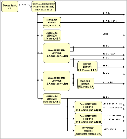
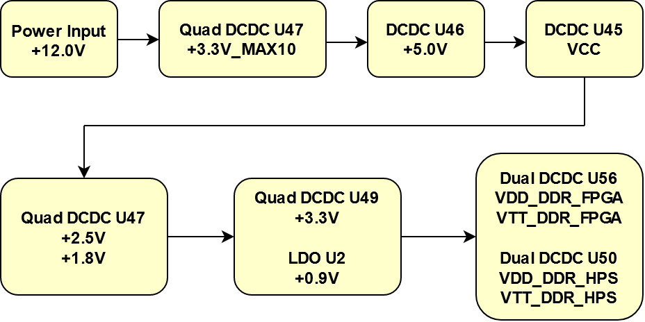
Power Distribution Dependencies
All on-board voltages of the TEI0022 are generated out of the extern applied 12 V power supply.
There are following dependencies how the initial 12V power supply is distributed to the on-board DC-DC converters, which power up further DCDC converters and the particular on-board voltages:
| Scroll Title | ||||||||||||||||||||||||||||||||
|---|---|---|---|---|---|---|---|---|---|---|---|---|---|---|---|---|---|---|---|---|---|---|---|---|---|---|---|---|---|---|---|---|
| ||||||||||||||||||||||||||||||||
|
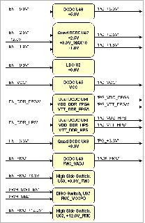
Power-On Sequence
The following figures delivers the power-on sequence information. The figure Power Sequency shows the connections between the power devices and its management. The figure Suggested Power Sequency shows the recommended firmware power-on sequence. For more information about firmware depended power-on sequencing see TEI0022 Intel MAX 10 → Power mangement.
| Scroll Title | ||||||||||||||||||||||||||||||||
|---|---|---|---|---|---|---|---|---|---|---|---|---|---|---|---|---|---|---|---|---|---|---|---|---|---|---|---|---|---|---|---|---|
| ||||||||||||||||||||||||||||||||
|
| Scroll Title | ||||||||||||||||||||||||||||||||
|---|---|---|---|---|---|---|---|---|---|---|---|---|---|---|---|---|---|---|---|---|---|---|---|---|---|---|---|---|---|---|---|---|
| ||||||||||||||||||||||||||||||||
|
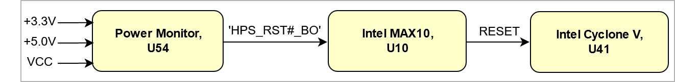
Voltage Monitor Circuit
The voltages +3.3V, +5.0V, and VCC are monitored by the voltage monitor circuit LTC2911 (U54), which generates a reset signal at power-on. A manual reset is also possible as described in the reset table.
| Scroll Title | ||||||||||||||||||||||||||||||||
|---|---|---|---|---|---|---|---|---|---|---|---|---|---|---|---|---|---|---|---|---|---|---|---|---|---|---|---|---|---|---|---|---|
| ||||||||||||||||||||||||||||||||
|
Bank Voltages
| Scroll Title | ||||||||||||||||||||||||||||||||||||||||||||||||||||||||||||||||||||||||||
|---|---|---|---|---|---|---|---|---|---|---|---|---|---|---|---|---|---|---|---|---|---|---|---|---|---|---|---|---|---|---|---|---|---|---|---|---|---|---|---|---|---|---|---|---|---|---|---|---|---|---|---|---|---|---|---|---|---|---|---|---|---|---|---|---|---|---|---|---|---|---|---|---|---|---|
| ||||||||||||||||||||||||||||||||||||||||||||||||||||||||||||||||||||||||||
|
Technical Specifications
| Scroll Ignore | ||||||||||||||||
|---|---|---|---|---|---|---|---|---|---|---|---|---|---|---|---|---|
| ||||||||||||||||
| Page properties | ||||
|---|---|---|---|---|
| ||||
List of all Powerrails which are accessible by the customer
|
Power Supply
The maximum power consumption of this board mainly depends on the design which is running on the FPGA. Intel provides a power estimator excel sheets to calculate power consumption.
Power Consumption
...
| anchor | Table_PWR_PC |
|---|---|
| title | Power Consumption |
...
* TBD - To Be Determined
Power Distribution Dependencies
All on-board voltages of the TEI0022 are generated out of the extern applied 12 V power supply.
There are following dependencies how the initial 12V power supply is distributed to the on-board DC-DC converters, which power up further DCDC converters and the particular on-board voltages:
...
| anchor | Figure_PWR_PD |
|---|---|
| title | Power Distribution |
| Scroll Ignore |
|---|
Create DrawIO object here: Attention if you copy from other page, objects are only linked. |
| Scroll Only |
|---|
image link to the generate DrawIO PNG file of this page. This is a workaround until scroll pdf export bug is fixed |
Power-On Sequence
...
| anchor | Figure_PWR_PS |
|---|---|
| title | Power Sequency |
| Scroll Ignore |
|---|
Create DrawIO object here: Attention if you copy from other page, objects are only linked. |
| Scroll Only |
|---|
image link to the generate DrawIO PNG file of this page. This is a workaround until scroll pdf export bug is fixed |
Voltage Monitor Circuit
...
| anchor | Figure_PWR_VMC |
|---|---|
| title | Voltage Monitor Circuit |
| Scroll Ignore |
|---|
Create DrawIO object here: Attention if you copy from other page, objects are only linked. |
| Scroll Only |
|---|
image link to the generate DrawIO PNG file of this page. This is a workaround until scroll pdf export bug is fixed |
Power Rails
...
| anchor | Table_PWR_PR |
|---|---|
| title | Module power rails. |
...
B2B Connector
JM1 Pin
...
B2B Connector
JM2 Pin
...
B2B Connector
JM3 Pin
...
Bank Voltages
...
| anchor | Table_PWR_BV |
|---|---|
| title | Zynq SoC bank voltages. |
...
Bank
...
Voltage
...
| hidden | true |
|---|---|
| id | Comments |
...
use "include page" macro and link to the general B2B connector page of the module series,
...
? x ? modules use two or three Samtec Micro Tiger Eye Connector on the bottom side.
3 x REF-??????? (compatible to ????????), (?? pins, ?? per row)
Operating Temperature: -??°C ~ ??°C
Current Rating: ??A per ContactNumber of Positions: ??
Number of Rows: ??
...
...
...
...
...
...
...
...
...
...
| Note |
|---|
For more information regarding how to draw diagram, Please refer to "Diagram Drawing Guidline" . |
.6/TE0745/REV02/Documents/AD-TE0745-02-30-1I.PDF
|
| Scroll Title | |||||||||||||||||||||||||||||||||||||||||||||||
|---|---|---|---|---|---|---|---|---|---|---|---|---|---|---|---|---|---|---|---|---|---|---|---|---|---|---|---|---|---|---|---|---|---|---|---|---|---|---|---|---|---|---|---|---|---|---|---|
| |||||||||||||||||||||||||||||||||||||||||||||||
|
Currently Offered Variants
| Scroll Ignore | ||
|---|---|---|
|
...
| anchor | Figure_TS_PD |
|---|---|
| title | Physical Dimension |
| Scroll Ignore |
|---|
Create DrawIO object here: Attention if you copy from other page, objects are only linked. |
...
...
Currently Offered Variants
...
...
...
...
...
...
Create DrawIO object here: Attention if you copy from other page, objects are only linked.
...
|

Document Change History
| Page properties | ||||
|---|---|---|---|---|
| ||||
|
...
...
| anchor | Table_RH_DCH |
|---|---|
| title | Document change history. |
...
...
...
| Page info | ||||||
|---|---|---|---|---|---|---|
|
...
change list
...
--
...
all
...
| Page info | ||||||
|---|---|---|---|---|---|---|
|
...
- --
...
Overview
Content Tools