...
| Scroll Title |
|---|
| anchor | Figure_OV_BD |
|---|
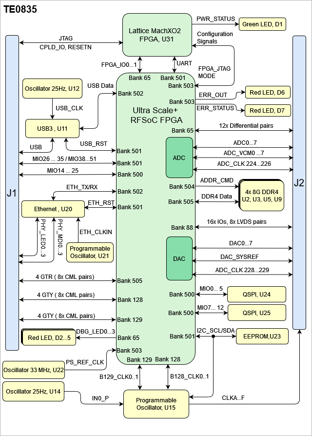
| title | TE0835 block diagram |
|---|
|
| Scroll Ignore |
|---|
| draw.io Diagram |
|---|
| border | false |
|---|
| viewerToolbar | true |
|---|
| |
|---|
| fitWindow | false |
|---|
| diagramDisplayName | |
|---|
| lbox | true |
|---|
| revision | 23 |
|---|
| diagramName | TE0835_OV_BD |
|---|
| simpleViewer | false |
|---|
| width | |
|---|
| links | auto |
|---|
| tbstyle | hidden |
|---|
| diagramWidth | 641 |
|---|
|
|
| Scroll Only |
|---|
|
|
...
| Scroll Title |
|---|
| anchor | Table_SIP_B2B |
|---|
| title | General PL I/O to B2B connectors information |
|---|
|
| Scroll Table Layout |
|---|
| orientation | portrait |
|---|
| sortDirection | ASC |
|---|
| repeatTableHeaders | default |
|---|
| style | |
|---|
| widths | |
|---|
| sortByColumn | 1 |
|---|
| sortEnabled | false |
|---|
| cellHighlighting | true |
|---|
|
B2B ConnectorInterface| B2B Connector | Number of I/Os | Voltage Level | Notes |
|---|
|
...
JTAG access to the TExxxx SoM through B2B connector JMX.
...
| anchor | Table_SIP_JTG |
|---|
| title | JTAG pins connection |
|---|
...
JTAG Signal
...
B2B Connector
...
| 500 | J1 | 12x Single Ended | 1.8V | MIO14...25 | | 501 | J1 | 20x Single Ended | 1.8V | MIO26...51 | | 505 | J1 | 18x Single Ended, 9x Differential pairs | 0.85V | EXT_CLKIN_PSMGT, RX/TX0...3 | | 128 | J1 | 18x Single Ended, 9x Differential pairs | 0.9V | B128_CLK, RX/TX0...3 | | 129 | J1 | 18x Single Ended, 9x Differential pairs | 0.9V | B129_CLK, RX/TX0...3 | | 65 | J2 | 24x Single Ended, 12x Differential pairs | 1.8V |
| | 88 | J2 | 16x Single Ended, 8x Differential pairs | 3.3V | HD_B88 |
|
JTAG Interface
JTAG access to the TE0835 is through B2B connector JM1.
| Scroll Title |
|---|
| anchor | Table_SIP_JTG |
|---|
| title | JTAG pins connection |
|---|
|
| Scroll Table Layout |
|---|
| orientation | portrait |
|---|
| sortDirection | ASC |
|---|
| repeatTableHeaders | default |
|---|
| style | |
|---|
| widths | |
|---|
| sortByColumn | 1 |
|---|
| sortEnabled | false |
|---|
| cellHighlighting | true |
|---|
|
JTAG Signal | B2B Connector |
|---|
| JTAG_TMS | J1-24 | | JTAG_TDI | J1-20 | | JTAG_TDO | J1-18 | | JTAG_TCK | J1-22 |
|
MIO Pins
| Page properties |
|---|
|
you must fill the table below with group of MIOs which are connected to a specific components or peripherals, you do not have to specify pins in B2B, Just mention which B2B is connected to MIOs. The rest is clear in the Schematic. Example: | MIO Pin | Connected to | B2B | Notes |
|---|
| MIO12...14 | SPI_CS , SPI_DQ0... SPI_DQ3 SPI_SCK | J2 | QSPI |
|
| Scroll Title |
|---|
| anchor | Table_OBP_MIOs |
|---|
| title | MIOs pins |
|---|
|
| Scroll Table Layout |
|---|
| orientation | portrait |
|---|
| sortDirection | ASC |
|---|
| repeatTableHeaders | default |
|---|
| style | |
|---|
| widths | |
|---|
| sortByColumn | 1 |
|---|
| sortEnabled | false |
|---|
| cellHighlighting | true |
|---|
|
| MIO Pin | Connected to | B2B | Notes |
|---|
| MIO0...12 | SPI FLash, U24-U25 | - | Dual SPI FLash | | MIO13 | LED Green, D1 | - | 3.3V_CPLD | | MIO14...25 | FPGA Bank 500,U1 | J1 | PSMIO | | MIO26...27 | FPGA Bank 501,U1 | J1 | PSMIO | | MIO28...29 | CPLD, U31 | - | UART_TX, UART_RX | | MIO30...31 | FPGA Bank 501, U1 | J1 | PSMIO | | MIO32...33 | EEPROM,U23 | - | I2C_SCL, I2C_SDA | | MIO34...35 | FPGA Bank 501,U1 | J1 | PSMIO | | MIO36 | Gigabit ETH, U20 | - | ETH_RST | | MIO37 | USB2.0, U11 | - | USB_RST | | MIO38...51 | FPGA Bank 501, U1 | J1 | PSMIO | | MIO52...62 | USB2.0, U11 | - | USB | | MIO63...77 | Gigabit ETH, U20 | - | ETH |
|
Test Points
...
| Page properties |
|---|
|
you must fill the table below with group of MIOs Test Point which are connected to a specific components or peripherals, you do not have to specify pins in B2B, Just mention which B2B is connected to MIOs. The rest is clear in the Schematicindicated as TP in a schematic. If there is no Test Point remarked in the schematic, delet the Test Point section. Example: | Test Point | Signal | MIO Pin | Connected to | B2B | Notes |
|---|
| MIO12...14 | SPI_CS , SPI_DQ0... SPI_DQ3 SPI_SCK | J2 | QSPI | | 10 | PWR_PL_OK | J2-120 |
|
|
| Scroll Title |
|---|
| anchor | Table_OBPSIP_MIOsTPs |
|---|
| title | MIOs pinsTest Points Information |
|---|
|
| Scroll Table Layout |
|---|
| orientation | portrait |
|---|
| sortDirection | ASC |
|---|
| repeatTableHeaders | default |
|---|
| style | |
|---|
| widths | |
|---|
| sortByColumn | 1 |
|---|
| sortEnabled | false |
|---|
| cellHighlighting | true |
|---|
|
|
...
|
| Page properties |
|---|
|
you must fill the table below with group of Test Point which are indicated as TP in a schematic. If there is no Test Point remarked in the schematic, delet the Test Point section.
Example:
| CLKOUT | Voltage Regulator, U7 |
| | TP2 | PLL_RSTN | Programmable Clock Generator, U15 |
| | TP3 | 3.3V_CPLD |
|
| | TP4 | CPLD_JTAGEN |
|
| | TP5 | JTAG_TDO |
|
| | TP6 | JTAG_TDI |
|
| | TP7 | JTAG_TCK |
|
| | TP8 | JTAG_TMS |
|
| | TP9 | GND |
|
| | TP10...11 | IO_L1P_AD15P_88, O_L4N_AD12N_88 | FPGA Bank 88, U1 |
| | TP12 | VIN | B2B, J1 |
| | TP13...14 | GND |
|
| | TP15...16 | MIO32-MIO33 | EEPROM,U23 FPGA Bank 501, U1 |
| | TP17 | GND |
|
| | TP18 | ADC_AVCC | LDO Voltage Regulator, U8 |
| | TP19 | ADC_AVCCAUX | LDO Voltage Regulator, U10 |
|
| Test Point | Signal | B2B | Notes |
|---|
10 | PWR_PL_OK | J2-120 | | Scroll Title |
|---|
| anchor | Table_SIP_TPs |
|---|
| title | Test Points Information |
|---|
|
| Scroll Table Layout |
|---|
|
| orientation | portrait |
|---|
| sortDirection | ASC |
|---|
| repeatTableHeaders | default |
|---|
style | widths | | sortByColumn | 1 |
|---|
| sortEnabled | false |
|---|
| cellHighlighting | true |
|---|
On-board Peripherals
| Page properties |
|---|
|
Notes : - add subsection for every component which is important for design, for example:
- Two 100 Mbit Ethernet Transciever PHY
- USB PHY
- Programmable Clock Generator
- Oscillators
- eMMCs
- RTC
- FTDI
- ...
- DIP-Switches
- Buttons
- LEDs
|
...
| Scroll Title |
|---|
| anchor | Table_OBP |
|---|
| title | On board peripherals |
|---|
|
| Scroll Table Layout |
|---|
| orientation | portrait |
|---|
| sortDirection | ASC |
|---|
| repeatTableHeaders | default |
|---|
| style | |
|---|
| widths | |
|---|
| sortByColumn | 1 |
|---|
| sortEnabled | false |
|---|
| cellHighlighting | true |
|---|
|
| Chip/Interface | Designator | Notes |
|---|
| SPI Flash | U24, U25 |
| | DDR4 SDRAM | U2, U3, U5, U9 |
| | CPLD | U31 |
| | USB2.0 | U11 |
| | Gigabit Ethernet | U20 |
| | Programmable Clock Generator | U15 |
| | EEPROM | U22 |
| | Oscillators | U14, U21, U12 |
| | LEDs | D0...7 |
|
|
Quad SPI Flash Memory
| Page properties |
|---|
|
Notes : Minimum and Maximum density of quad SPI flash must be mentioned for other assembly options. |
...
| Scroll Title |
|---|
| anchor | Table_OBP_SPI |
|---|
| title | Quad SPI interface MIOs and pins |
|---|
|
| Scroll Table Layout |
|---|
| orientation | portrait |
|---|
| sortDirection | ASC |
|---|
| repeatTableHeaders | default |
|---|
| style | |
|---|
| widths | |
|---|
| sortByColumn | 1 |
|---|
| sortEnabled | false |
|---|
| cellHighlighting | true |
|---|
|
| MIO Pin | Schematic | U?? U24 Pin | Notes |
|---|
|
|
|
|
|
|
|
|
|
|
|
|
|
|
|
|
|
|
|
|
|
|
|
|
|
RTC
| Scroll Title |
|---|
| anchor | Table_OBP_RTC |
|---|
| title | I2C interface MIOs and pins |
|---|
|
| Scroll Table Layout |
|---|
| orientation | portrait |
|---|
| sortDirection | ASC |
|---|
| repeatTableHeaders | default |
|---|
| style | |
|---|
| widths | |
|---|
| sortByColumn | 1 |
|---|
| sortEnabled | false |
|---|
| cellHighlighting | true |
|---|
|
| MIO Pin | Schematic | U? Pin | Notes |
|---|
|
|
|
|
|
|
|
|
|
...